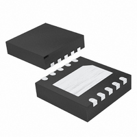
MAX15024BATB+T Maxim Integrated Products, MAX15024BATB+T Datasheet

MAX15024BATB+T
Specifications of MAX15024BATB+T
Related parts for MAX15024BATB+T
MAX15024BATB+T Summary of contents
Page 1
... CMOS or TTL Logic-Level Inputs with Hysteresis for Noise Immunity o -40°C to +125°C Operating Temperature Range o Thermal-Shutdown Protection o 1.95W Thermally Enhanced TDFN Power Packages Applications PART MAX15024AATB+T MAX15024BATB+T MAX15025AATB+T MAX15025BATB+T MAX15025CATB+T MAX15025DATB+T 6 Note: All devices are specified over the -40°C to +125°C operating temperature range. ...
Page 2
Single/Dual, 16ns, High Sink/Source Current Gate Drivers ABSOLUTE MAXIMUM RATINGS V to GND ............................................................-0.3V to +30V CC REG to GND ..............-0.3V to the lower of +22V or (V DRV to PGND .........................................................-0.3V to +22V IN_ ..........................................................................-0.3V to +22V FB/SET to ...
Page 3
Single/Dual, 16ns, High Sink/Source MAX15024 ELECTRICAL CHARACTERISTICS (continued 10V, FB/SET = GND DRV REG + 25°C). (Note 2) PARAMETER SYMBOL DRIVER OUTPUT (SINK) Driver Output Resistance R Peak Output Current I Maximum ...
Page 4
Single/Dual, 16ns, High Sink/Source Current Gate Drivers MAX15024 ELECTRICAL CHARACTERISTICS (continued 10V, FB/SET = GND DRV REG + 25°C). (Note 2) PARAMETER SYMBOL SWITCHING CHARACTERISTICS FOR V Rise Time Fall Time Turn-On ...
Page 5
Single/Dual, 16ns, High Sink/Source MAX15025 ELECTRICAL CHARACTERISTICS (continued 10V, FB/SET = GND DRV REG +25°C). (Note 2) PARAMETER SYMBOL V Undervoltage-Lockout CC Hysteresis V Undervoltage Lockout to CC Output Delay REG REGULATOR ...
Page 6
Single/Dual, 16ns, High Sink/Source Current Gate Drivers MAX15025 ELECTRICAL CHARACTERISTICS (continued 10V, FB/SET = GND DRV REG +25°C). (Note 2) PARAMETER SYMBOL SWITCHING CHARACTERISTICS FOR V Rise Time Fall Time Turn-On Delay ...
Page 7
Single/Dual, 16ns, High Sink/Source (T = +25°C, unless otherwise noted.) A RISE TIME vs. SUPPLY VOLTAGE (DUAL DRIVER WITH 5nF LOAD) 40 MAX15025 T = +125° +85° +25° 0°C ...
Page 8
Single/Dual, 16ns, High Sink/Source Current Gate Drivers (T = +25°C, unless otherwise noted.) A LOGIC INPUT VOLTAGE vs. OUTPUT VOLTAGE (5nF FALLING) MAX15024/25 toc10 MAX15025 IN_ 1V/div OUT_ 5V/div 20ns/div PROPAGATION DELAY MISMATCH vs. TEMPERATURE 3.0 2.5 2.0 1.5 1.0 ...
Page 9
Single/Dual, 16ns, High Sink/Source PIN MAX15025A MAX15025C MAX15024 MAX15025B MAX15025D — — — — — — 5 — — — — — ...
Page 10
Single/Dual, 16ns, High Sink/Source Current Gate Drivers Detailed Description The MAX15024 single gate driver’s internal source and sink transistor outputs are brought out of the IC to inde- pendent outputs allowing control of the external MOSFET’s rise and fall time. ...
Page 11
Single/Dual, 16ns, High Sink/Source Power Dissipation Power dissipation of the MAX15024/MAX15025 con- sists of three components: the quiescent current, capacitive charge and discharge of internal nodes, and the output current (either capacitive or resistive load). The sum of these components ...
Page 12
Single/Dual, 16ns, High Sink/Source Current Gate Drivers REG DRV R2 MAX15024 FB/SET P_OUT R1 N_OUT V CC (UP TO 28V PGND GND IN- IN+ Figure 2. Use R1 program V REG FB/SET to GND for V ...
Page 13
Single/Dual, 16ns, High Sink/Source V CC UVLO FB/SET IN_ LOGIC LEVEL SHIFT-UP IN+ IN- IN_ LOGIC LEVEL SHIFT-UP GND V CC UVLO FB/SET LEVEL SHIFT-UP IN1 LEVEL SHIFT-UP IN_ LOGIC LEVEL SHIFT-UP IN2 IN_ LOGIC GND LEVEL SHIFT-UP ______________________________________________________________________________________ Current ...
Page 14
Single/Dual, 16ns, High Sink/Source Current Gate Drivers NO. OF PART CHANNELS MAX15024AATB+ 1 MAX15024BATB+ 1 MAX15025AATB+ 2 MAX15025BATB+ 2 MAX15025CATB+ 2 MAX15025DATB+ 2 Note: All devices operate in a -40°C to +125°C temperature range and come in a 10-pin TDFN ...
Page 15
Single/Dual, 16ns, High Sink/Source Chip Information PROCESS: BiCMOS ______________________________________________________________________________________ Current Gate Drivers Package Information For the latest package outline information and land patterns www.maxim-ic.com/packages. Note that a “+”, “#”, or “-” in the package code indicates RoHS status ...
Page 16
... Maxim cannot assume responsibility for use of any circuitry other than circuitry entirely embodied in a Maxim product. No circuit patent licenses are implied. Maxim reserves the right to change the circuitry and specifications without notice at any time. 16 ____________________Maxim Integrated Products, 120 San Gabriel Drive, Sunnyvale, CA 94086 408-737-7600 © 2010 Maxim Integrated Products DESCRIPTION Maxim is a registered trademark of Maxim Integrated Products, Inc ...


