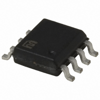
MIC5013BM Micrel Inc, MIC5013BM Datasheet - Page 6

MIC5013BM
Manufacturer Part Number
MIC5013BM
Description
IC DRIVER MOSF HI/LO SIDE 8SOIC
Manufacturer
Micrel Inc
Datasheet
1.MIC5013YM.pdf
(15 pages)
Specifications of MIC5013BM
Configuration
High or Low Side
Input Type
Non-Inverting
Delay Time
60µs
Number Of Configurations
1
Number Of Outputs
1
Voltage - Supply
7 V ~ 32 V
Operating Temperature
-40°C ~ 85°C
Mounting Type
Surface Mount
Package / Case
8-SOIC (3.9mm Width)
Number Of Drivers
1
Driver Type
High Side/Low Side
Operating Supply Voltage (max)
32V
Power Dissipation
1.25W
Operating Supply Voltage (min)
7V
Operating Supply Voltage (typ)
15V
Turn Off Delay Time
4us
Turn On Delay Time (max)
60us
Operating Temp Range
-40C to 85C
Operating Temperature Classification
Industrial
Mounting
Surface Mount
Pin Count
8
Package Type
SOIC
Lead Free Status / RoHS Status
Contains lead / RoHS non-compliant
Current - Peak
-
High Side Voltage - Max (bootstrap)
-
Lead Free Status / Rohs Status
Not Compliant
Available stocks
Company
Part Number
Manufacturer
Quantity
Price
Part Number:
MIC5013BM
Manufacturer:
MICREL
Quantity:
20 000
Company:
Part Number:
MIC5013BM/YM
Manufacturer:
MICREL
Quantity:
300
MIC5013
Block Diagram
Applications Information
Functional Description (refer to block diagram)
The various MIC5013 functions are controlled via a logic
block connected to the input pin 1. When the input is low,
all functions are turned off for low standby current and the
gate of the power MOSFET is also held low through 500Ω
to an N-channel switch. When the input is taken above the
turn-on threshold (3.5V typical), the N-channel switch turns
off and the charge pump is turned on to charge the gate of
the power FET. A bandgap type voltage regulator is also
turned on which biases the current sense circuitry.
The charge pump incorporates a 100kHz oscillator and
on-chip pump capacitors capable of charging 1nF to 5V
above supply in 60µs typical. The charge pump is capable
of pumping the gate up to over twice the supply voltage.
For this reason, a zener clamp (12.5V typical) is provided
between the gate pin 6 and source pin 4 to prevent exceed-
ing the V
The current sense operates by comparing the sense volt-
age at pin 3 to an offset version of the source voltage at
pin 4. Current I2 flowing in threshold pin 2 is mirrored and
returned to the source via a 1kΩ resistor to set the offset,
or trip voltage. When (V
the current sense trips and sets the current sense latch to
turn off the power FET. An integrating comparator is used
to reduce sensitivity to spikes on pin 3. The latch is reset
to turn the FET back on by “recycling” the input pin 1 low
and then high again.
A resistor R
An additional capacitor C
higher trip voltage at turn-on, which is necessary to prevent
high in-rush current loads such as lamps or capacitors from
false-tripping the current sense.
MIC5013
GS
TH
rating of the MOSFET at high supplies.
from pin 2 to ground sets I2, and hence V
Input
Fault
1
8
SENSE
TH
from pin 2 to ground creates a
– V
LOGIC
SOURCE
Ground
V+
5
7
CURRENT
) exceeds V
SENSE
LATCH
Q
V. REG
S
R
TRIP
TRIP
MIC5013
,
.
6
+
–
When the current sense has tripped, the fault pin 8 will be
high as long as the input pin 1 remains high. However, when
the input is low the fault pin will also be low.
Construction Hints
High current pulse circuits demand equipment and assembly
techniques that are more stringent than normal low current
lab practices. The following are the sources of pitfalls most
often encountered during prototyping: Supplies: many bench
power supplies have poor transient response. Circuits that
are being pulse tested, or those that operate by pulse-width
modulation will produce strange results when used with a
supply that has poor ripple rejection, or a peaked transient
response. Monitor the power supply voltage that appears
at the drain of a high-side driver (or the supply side of the
load in a low-side driver) with an oscilloscope. It is not un-
common to find bench power supplies in the 1kW class that
overshoot or undershoot by as much as 50% when pulse
loaded. Not only will the load current and voltage measure-
ments be affected, but it is possible to over-stress various
components—especially electrolytic capacitors—with pos-
sibly catastrophic results. A 10µF supply bypass capacitor
at the chip is recommended.
Residual Resistances: Resistances in circuit connections
may also cause confusing results. For example, a circuit
may employ a 50mΩ power MOSFET for low drop, but
careless construction techniques could easily add 50 to
100mΩ resistance. Do not use a socket for the MOSFET. If
the MOSFET is a TO-220 type package, make high-current
drain connections to the tab. Wiring losses have a profound
effect on high-current circuits. A floating millivoltmeter can
identify connections that are contributing excess drop
under load.
Threshold
2
CHARGE
PUMP
1k
I2
V+
V
TR I P
–
+
1k
500Ω
12.5V
6
3
4
Gate
Sense
Source
July 2005
Micrel, Inc.


