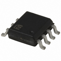
MIC4421ABM Micrel Inc, MIC4421ABM Datasheet - Page 7

MIC4421ABM
Manufacturer Part Number
MIC4421ABM
Description
IC DRIVER MOSFET 9A LS 8-SOIC
Manufacturer
Micrel Inc
Datasheet
1.MIC4421AZM.pdf
(13 pages)
Specifications of MIC4421ABM
Configuration
Low-Side
Input Type
Inverting
Delay Time
15ns
Current - Peak
9A
Number Of Configurations
1
Number Of Outputs
1
Voltage - Supply
4.5 V ~ 18 V
Operating Temperature
-40°C ~ 85°C
Mounting Type
Surface Mount
Package / Case
8-SOIC (3.9mm Width)
Lead Free Status / RoHS Status
Contains lead / RoHS non-compliant
High Side Voltage - Max (bootstrap)
-
Functional Diagram
Functional Description
Refer to the functional diagram.
The MIC4422A is a non-inverting driver. A logic high on
the IN produces gate drive output. The MIC4421A is an
inverting driver. A logic low on the IN produces gate
drive output. The output is used to turn on an external N-
channel MOSFET.
Supply
V
capacitors are recommended to decouple noise.
Input
IN (control) is a TTL-compatible input. IN must be forced
high or low by an external signal. A floating input will
cause unpredictable operation.
A high input turns on Q1, which sinks the output of the
0.1mA and the 0.3mA current source, forcing the input of
the first inverter low.
Hysteresis
The control threshold voltage, when IN is rising, is
slightly higher than the control threshold voltage when
CTL is falling.
When IN is low, Q2 is on, which applies the additional
0.3mA current source to Q1. Forcing IN high turns on Q1
Micrel, Inc.
June 2007
S
(supply) is rated for +4.5V to +18V. External
IN
0.1mA
Q1
Figure 4. MIC4421A/22A Block Diagram
Q2
0.3mA
NONINVERTING
7
INVERTING
MIC4422A
MIC4421A
which must sink 0.4mA from the two current sources.
The higher current through Q1 causes a larger drain-to-
source voltage drop across Q1. A slightly higher control
voltage is required to pull the input of the first inverter
down to its threshold.
Q2 turns off after the first inverter output goes high. This
reduces the current through Q1 to 0.1mA. The lower
current reduces the drain-to-source voltage drop across
Q1. A slightly lower control voltage will pull the input of
the first inverter up to its threshold.
Drivers
The second (optional) inverter permits the driver to be
manufactured in inverting and non-inverting versions.
The last inverter functions as a driver for the output
MOSFETs Q3 and Q4.
Output
OUT is designed to drive a capacitive load. V
voltage) is either approximately the supply voltage or
approximately ground, depending on the logic state
applied to IN.
If IN is high, and V
will be floating (unpredictable).
Q3
Q4
S
GND
(supply) drops to zero, the output
VS
OUT
MIC4421A/4422A
M9999-062707
OUT
(output


