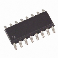
T6819-TBQ Atmel, T6819-TBQ Datasheet

T6819-TBQ
Specifications of T6819-TBQ
Related parts for T6819-TBQ
T6819-TBQ Summary of contents
Page 1
... SO16 Power Package Description The T6819/T6829 are fully protected driver interfaces designed in 0.8-µm BCDMOS technology. They are used to control up to six different loads by a microcontroller in automotive and industrial applications. Each of the three high-side and three low-side drivers is capable to drive currents ...
Page 2
... Figure 1. Block Diagram OUT3H 4 Fault detect CLK Input register Output register PWM Fault detect 3 OUT3L T6819/T6829 [Preliminary] 2 OUT2H OUT1H 14 Fault Fault detect detect Serial interface Fault Fault detect detect 15 OUT2L OUT1L 13 Charge pump Control protection logic Power-on reset Thermal protection 2 12 ...
Page 3
... Pin Configuration Figure 2. Pinning SO16 Pin Description Pin Symbol Function T6819: ground; reference potential; internal connection to pin 9 and pin 16; cooling tab 1 GND T6829: additional connection to heat slug Low-side driver output 1; power MOS open drain with internal reverse diode; short-circuit protection; 2 OUT1L overtemperature protection ...
Page 4
... DO TP S1L S1H T6819/T6829 [Preliminary] 4 Data transfer starts with the falling edge of the CS signal. Data must appear at DI syn- chronized to CLK and are accepted on the falling edge of the CLK signal. LSB (bit 0, SRR) has to be transferred first. Execution of new input data is enabled on the rising edge of the CS signal ...
Page 5
... High = standby, low = normal operation 15 PSF Power-supply fail: undervoltage at pin VS detected Bit 11 Bit 10 Bit 9 Bit 8 Bit 7 PL3 PH2 PL2 PH1 PL1 Bit 10 Bit 9 Bit 8 Bit T6819/T6829 [Preliminary] Bit 6 Bit 5 Bit 4 Bit 3 HS3 LS3 HS2 LS2 Bit 6 Bit 5 Bit 4 Bit 3 (HS3) (LS3) (HS2) (LS2 ...
Page 6
... OVL bit is not set by an overcurrent. By writing a high to the SRR bit in the input register the OVL bit is reset and the disabled outputs are enabled. The SI bit in the input register has to be set to zero to inhibit the T6819/T6829. All output stages are then turned off but the serial interface stays active. The current consumption is reduced to less than 5 µ ...
Page 7
... Out1H Out3L Out2L, Out1L STG Symbol VCC CLK PWM f CLK f PWM T j T6819/T6829 [Preliminary] Value -0.3 to + 0.3 VCC -0 0.3 VCC -10 to +10 -10 to +10 -0.3 to +40 17 -40 to +150 -55 to +150 Symbol Value R 30 thJP R 65 thJA R 5 thJP R 30 thJA ...
Page 8
... Device not in standby for t > 1 ms. 2. Delay time between rising/falling edge of input signal at pin PWM and switch on/off output stages to 90% of final level. 3. Difference between switch-on and switch-off delay time of input signal at pin PWM to output stages in PWM mode. T6819/T6829 [Preliminary] 8 Test Conditions ...
Page 9
... Out 1 13 Out1 - Ω Load = Ω Load = Ω Load T6819/T6829 [Preliminary] Min. Typ. Max. 135 160 185 j switch switch off j switch off/ 1.05 1.2 jPW set j switch on/ 1.05 1.2 jPW reset 1.1 DSOn1-3H 1.1 DSOn1-3L -5 Out1-3H I Out1- 1.5 VS -1.5 Out1-3L -2 ...
Page 10
... Delay time between rising/falling edge of input signal at pin PWM and switch on/off output stages to 90% of final level. 3. Difference between switch-on and switch-off delay time of input signal at pin PWM to output stages in PWM mode. T6819/T6829 [Preliminary] 10 < 150° C; unless otherwise specified, all values refer to GND pins. ...
Page 11
... CLK period time 8.12 CLK setup time 8.13 CLK setup time 8.14 DI setup time 8.15 DI hold time *) Type means: A =100% tested 100% correlation tested Characterized on samples Design parameter Note: 1. See Figure 4 on page 12 4531D–BCD–07/04 T6819/T6829 [Preliminary] (1) Pin Timing Chart No. Symbol ENDO ...
Page 12
... Figure 4. Serial Interface Timing with Chart Number CLK 3 DI CLK DO Inputs DI, CLK, CS: High level = 0.7 × V Output DO: High level = 0.8 × V T6819/T6829 [Preliminary low level = 0.3 × low level = 0.2 × 4531D–BCD–07/04 ...
Page 13
... Negative spikes at the output pins (e.g. negative spikes caused by an inductive load switched off with a high side driver) may activate the overtemperature protection func- tion of the T6819/T6829. In this condition, the affected output will be switched off. If this behavior is not acceptable or compatible with the specific application functionally necessary, that for switching on required outputs again, the SRR bit ( S tatus R egister R eset) is set, to ensure a reset of the overtemperature function ...
Page 14
... Ordering Information Extended Type Number Package T6819-TBS T6819-TBQ T6829-T3S T6829-T3Q Package Information Package SO16 Dimensions in mm T6819/T6829 [Preliminary] 14 Remarks SO16 Power package, tubed SO16 Power package, taped and reeled SO16 Power package with heat slug, tubed SO16 Power package with heat slug, taped and reeled 10 ...
Page 15
... Revision History Changes from Rev. 4531C - 04/04 to Rev. 4531D - 07/04 4531D–BCD–07/04 Please note that the following page numbers referred to in this section refer to the specific revision mentioned, not to this document. 1. Table “Ordering Information” on page 14 changed. T6819/T6829 [Preliminary] 15 ...
Page 16
... No licenses to patents or other intellectual property of Atmel are granted by the Company in connection with the sale of Atmel products, expressly or by implication. Atmel’s products are not authorized for use as critical components in life support devices or systems. ...


