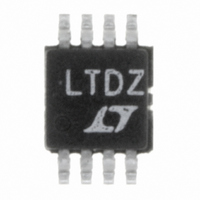
LTC1710CMS8#TR Linear Technology, LTC1710CMS8#TR Datasheet - Page 4

LTC1710CMS8#TR
Manufacturer Part Number
LTC1710CMS8#TR
Description
IC SWITCH SMBUS DUAL HISD 8MSOP
Manufacturer
Linear Technology
Type
High Sider
Datasheet
1.LTC1710CS8.pdf
(8 pages)
Specifications of LTC1710CMS8#TR
Input Type
2-Wire SMBus
Number Of Outputs
2
On-state Resistance
400 mOhm
Current - Output / Channel
300mA
Current - Peak Output
1A
Voltage - Supply
2.7 V ~ 5.5 V
Operating Temperature
0°C ~ 70°C
Mounting Type
Surface Mount
Package / Case
8-MSOP, Micro8™, 8-uMAX, 8-uSOP,
Switch Type
High Side
Power Switch Family
LTC1710
Input Voltage
2.7 to 5.5V
Power Switch On Resistance
550mOhm
Mounting
Surface Mount
Supply Current
17uA
Package Type
MSOP
Operating Temperature (min)
0C
Operating Temperature (max)
70C
Operating Temperature Classification
Commercial
Pin Count
8
Lead Free Status / RoHS Status
Contains lead / RoHS non-compliant
Available stocks
Company
Part Number
Manufacturer
Quantity
Price
TYPICAL PERFOR A CE CHARACTERISTICS
PIN
LTC1710
SW0D (Pin 1): Drain Supply of Switch 0. User-program-
mable from 0V to V
OUT0 (Pin 2): Source Output of Switch 0. Maximum load
of 300mA; controlled by LSB of command byte.
AD1 (Pin 3): Three-State Programmable Address Pin.
Must be connected directly to V
two resistors 1M). Do not float this pin.
GND (Pin 4): Ground Connection.
4
0.6
1.0
0.9
0.8
0.7
0.5
0.4
0.3
0.2
0.1
50
40
30
20
10
U
0
0
– 50
– 50
Standby Current vs Temperature
Switch R
(SO-8 Package)
I
OUT
FUNCTIONS
= 300mA
U
V
V
CC
DS(ON)
V
CC
CC
TEMPERATURE ( C)
TEMPERATURE ( C)
= 2.7V
0
0
= 5V
= 3.3V
V
CC
vs Temperature
CC
= 3.3V
U
.
50
50
V
CC
V
W
CC
= 2.7V
= 5V
1710 G04
1710 G01
CC
U
100
100
, GND or V
500
400
300
200
100
1.0
0.9
0.8
0.7
0.6
0.5
0.4
0.3
0.2
0.1
0
0
– 50
CC
Supply Current (I
vs Temperature
Switch R
(MSOP Package)
0
V
I
OUT
/2 (using
CC
= 5V
= 300mA
20
DS(ON)
V
TEMPERATURE ( C)
TEMPERATURE ( C)
CC
0
BOTH SW ON
= 3.3V
40
SW1 ON
vs Temperature
Q
CLK (Pin 5): Serial Clock Interface. Must be pulled high to
V
limited to 350 A.
DATA (Pin 6): Open-Drain Connected Serial Data Inter-
face. Must be pulled high to V
pull-up current must be limited to 350 A.
OUT1 (Pin 7): Source Output of Switch 1. Maximum load
of 300mA; controlled by 2nd LSB of command byte.
V
2.7V to 5.5V.
)
CC
CC
60
50
(Pin 8): Input Supply Voltage. Operating range from
with external resistor. The pull-up current must be
SW0 ON
V
V
CC
CC
80
= 2.7V
= 5V
1710 G02
1710 G05
100
100
100
500
400
300
200
400
200
100
300
0
0
– 50
Supply Current (I
vs Supply Voltage
0
Data ACK V
T
I
A
PULL-UP
= 25 C
CC
with external resistor. The
= 350 A
2
SUPPLY VOLTAGE (V)
TEMPERATURE ( C)
OL
0
BOTH SW ON
vs Temperature
4
Q
)
50
SW1 ON
SW0 ON
6
1710 G03
1710 G06
100
8


