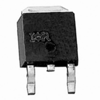
IPS1041RTRRPBF International Rectifier, IPS1041RTRRPBF Datasheet - Page 2

IPS1041RTRRPBF
Manufacturer Part Number
IPS1041RTRRPBF
Description
IC SWITCH IPS 1CH LOW SIDE DPAK
Manufacturer
International Rectifier
Type
Low Sider
Datasheet
1.IPS1042GPBF.pdf
(15 pages)
Specifications of IPS1041RTRRPBF
Input Type
Non-Inverting
Number Of Outputs
1
On-state Resistance
80 mOhm
Current - Output / Channel
2.2A
Current - Peak Output
4.5A
Voltage - Supply
4.5 V ~ 5.5 V
Operating Temperature
-40°C ~ 150°C
Mounting Type
Surface Mount
Package / Case
DPak, TO-252 (2 leads+tab), SC-63
Lead Free Status / RoHS Status
Lead free / RoHS Compliant
Absolute Maximum Ratings
Absolute maximum ratings indicate sustained limits beyond which damage to the device may occur. All voltage parameters
are referenced to Ground lead. (Tambient=25°C unless otherwise specified).
Thermal Characteristics
Recommended Operating Conditions
These values are given for a quick design. For operation outside
(
www.irf.com
1) Higher ind
Symbol
Rth1
Rth2
Rth1
Rth2
Rth1
Rth1
Symbol
VIH
VIL
Ids
Rin
Max L
Max. F
Max. t rise
Symbol
Vds
Vds cont
Vin
Isd cont.
Pd
ESD
Tj max.
Tsoldering
ucta
Parameter
Maximum drain to source voltage
Maximum continuous drain to sourc
Maximum input voltage
Max diode continuous cu
Maximum power dissipation (internally limited by thermal protection)
Electrostatic discharge voltage (Human body) C=100pF, R=1500Ω
Electrostatic discharge voltage (Machine Model) C=200pF,R=0Ω
M
Lead soldering temperature (10 seconds)
Parameter
Thermal resistance junction to ambient IPS1041L SOT-223 std. footprint
Thermal resistance junction to ambient IPS1041L SOT-223 1” sqr. footprint
Thermal resistance junction to ambient IPS1041R D-Pak std. footprint
Thermal resistance junction to case IPS1041R D-Pak
Thermal resistance junction to ambient IPS1042G SO-8 std. Footprint
Thermal resistance junction to ambient IPS1042G SO-8 std. footprint
nce is possible if maxim
Continuou
Parameter
Low level input voltage
Continuous drain current, Tambient=85°C, Tj=125°C, Vin=5V
Continuou
Continuous drain current, Tambient=85°C, Tj=125°C, Vin=5V
R
ax. storage & operating temperature junction temperature
High level input voltage
Max. recommended load inductance ( including line inductance ) (1)
Max. frequency
Max. input rising
ecomme
s drain current, Tambient=85°C, Tj=125°C
s drain current, Tambient=85°C, Tj=125°C
nded resistor in series with IN pin to generate a diagnost
Rth=100°C/W IPS1042G 1” sqr. Footprint - 1 die active
Rth=130°C/W IPS1042G 1” sqr. Footprint - 2 die act
Rth=60°C/W IPS1041L 1” sqr. Footprint
Rth=50°C/W IPS1041R 1” sqr. Footprint
time
rrent (limited by thermal dissipation)
um load current is limited - see figure 11
Rth=60°C/W IPS1041L 1” sqr. footprint
Rth=100°C/W IPS1042G std. footprint
Between drain and source
Other combinations
Between drain and source
Other combinations
IPS1041(L)(R)PbF / IPS1042GPbF
e voltage
these conditions, please consult the application notes.
, Vin=5V
, Vin=5V
ive
1 die active
2 die
ic
active
Typ.
Min.
Min.
-0.3
-0.3
100
100
130
-40
4.5
0.5
60
70
⎯
⎯
⎯
⎯
⎯
⎯
⎯
⎯
⎯
⎯
⎯
⎯
6
0
-
Max.
Max.
Max.
2000
1.25
1.95
150
300
1.5
0.5
0.3
5.5
0.5
2.2
1.5
0.7
28
36
10
20
⎯
⎯
⎯
⎯
⎯
⎯
6
2
4
3
1
Units
Units
°C/W
Un
2
µH
Hz
kV
°C
°C
k
µs
W
V
V
V
A
V
A
Ω
its


