NCV8401DTRKG ON Semiconductor, NCV8401DTRKG Datasheet
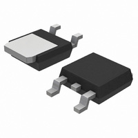
IC DVR LOSIDE 33A 42V DPAK-4

NCV8401DTRKG

Manufacturer Part Number
NCV8401DTRKG
Description
IC DVR LOSIDE 33A 42V DPAK-4
Manufacturer
ON Semiconductor
Type
Low Sider
Datasheet

Specifications of NCV8401DTRKG

Input Type
Non-Inverting
Number Of Outputs
1
On-state Resistance
23 mOhm
Current - Output / Channel
35A
Current - Peak Output
35A
Operating Temperature
-55°C ~ 150°C
Mounting Type
Surface Mount
Package / Case
DPak, TO-252 (2 leads+tab), SC-63
Configuration
Single
Transistor Polarity
N-Channel
Resistance Drain-source Rds (on)
0.029 Ohms
Drain-source Breakdown Voltage
42 V
Gate-source Breakdown Voltage
+/- 14 V
Power Dissipation
64 W
Maximum Operating Temperature
+ 150 C
Mounting Style
SMD/SMT
Minimum Operating Temperature
- 55 C
Operating Temperature (max)
150C
Operating Temperature (min)
-40C
Pin Count
2 +Tab
Mounting
Surface Mount
Package Type
DPAK
Screening Level
Automotive
Lead Free Status / RoHS Status
Lead free / RoHS Compliant
Voltage - Supply
-
Lead Free Status / Rohs Status
 Details

Available stocks

Company
Part Number
Manufacturer
Quantity
Price
Part Number:
NCV8401DTRKG
Manufacturer:
ON
Quantity:
5 000
Part Number:
NCV8401DTRKG
Manufacturer:
ON
Quantity:
12 500
Part Number:
NCV8401DTRKG
Manufacturer:
ON/安森美
Quantity:
20 000
NCV8401
Self-Protected Low Side
Driver with Temperature
and Current Limit
device. The protection features include overcurrent, overtemperature,
ESD and integrated Drain-to-Gate clamping for overvoltage protection.
This device offers protection and is suitable for harsh automotive
environments.
Features
Typical Applications
© Semiconductor Components Industries, LLC, 2010
February, 2010 − Rev. 7
NCV8401 is a three terminal protected Low-Side Smart Discrete
and Change Control
Short Circuit Protection
Thermal Shutdown with Automatic Restart
Over Voltage Protection
Integrated Clamp for Inductive Switching
ESD Protection
dV/dt Robustness
Analog Drive Capability (Logic Level Input)
RoHs Compliant
AEC-Q101 Qualified
NCV Prefix for Automotive and Other Applications Requiring Site
This is a Pb−Free Device
Switch a Variety of Resistive, Inductive and Capacitive Loads
Can Replace Electromechanical Relays and Discrete Circuits
Automotive / Industrial
1
*Max current may be limited below this value
Y
WW
xxx
G
†For information on tape and reel specifications,
NCV8401DTRKG
Gate
Input
depending on input conditions.
including part orientation and tape sizes, please
refer to our Tape and Reel Packaging Specification
Brochure, BRD8011/D.
(Clamped)
V
CASE 369C
42 V
Device
DSS
STYLE 2
DPAK
ESD Protection
= Year
= Work Week
= Device Code
= Pb−Free Package
ORDERING INFORMATION
Temperature
http://onsemi.com
Limit
23 mW @ 10 V
R
Overvoltage
Protection
DS(ON)
(Pb−Free)
Package
DPAK
Publication Order Number:
TYP
Current
Limit
1
3
2500/Tape & Reel
2
1 = Gate
2 = Drain
3 = Source
Shipping
MARKING
DIAGRAM
Drain
(Limited)
Current
xxxxxG
NCV8401/D
Sense
I
YWW
D
Source
33 A*
xxx
MAX

Related parts for NCV8401DTRKG

NCV8401DTRKG Summary of contents

Page 1

... STYLE Year WW = Work Week xxx = Device Code G = Pb−Free Package ORDERING INFORMATION Device Package NCV8401DTRKG DPAK (Pb−Free) †For information on tape and reel specifications, including part orientation and tape sizes, please refer to our Tape and Reel Packaging Specification Brochure, BRD8011/ MAX D (Limited) ...

Page 2

MAXIMUM RATINGS (T = 25°C unless otherwise noted) J Drain−to−Source Voltage Internally Clamped Drain−to−Gate Voltage Internally Clamped (R = 1.0 MW) GS Gate−to−Source Voltage Drain Current − Continuous Total Power Dissipation @ T = 25°C (Note ...

Page 3

MOSFET ELECTRICAL CHARACTERISTICS Characteristic OFF CHARACTERISTICS Drain−to−Source Clamped Breakdown Voltage ( Vdc 250 mAdc Vdc 250 mAdc Zero Gate Voltage Drain Current ( Vdc, ...

Page 4

T = 25°C Jstart 150°C Jstart (mH) Figure 2. Single Pulse Maximum Switch−off Current vs. Load Inductance 100 T = 25°C Jstart 150°C Jstart 1 1 Time in Clamp (ms) ...

Page 5

V (V) GS Figure 8. R vs. Gate−Source Voltage DS(on) 2.00 1.75 1.50 1. 1.00 0. ...

Page 6

TYPICAL PERFORMANCE CURVES 1.2 1.1 1.0 0.9 0.8 0.7 0.6 −40 − (°C) Figure 14. Normalized Threshold Voltage vs. Temperature (I = 1.2 mA 200 150 100 50 t d(on ...

Page 7

Duty Cycle 10 0.1 0.01 Single Pulse 0.001 1E−06 0.00001 0.0001 Figure 21. Transient Thermal Resistance TYPICAL PERFORMANCE CURVES PCB Cu thickness, ...

Page 8

TEST CIRCUITS AND WAVEFORMS VIN RG Figure 22. Resistive Load Switching Test Circuit VIN td(ON) tr IDS Figure 23. Resistive Load Switching Waveforms http://onsemi.com VDD − DUT G S IDS td(OFF 90% 10% 90% 10% ...

Page 9

TEST CIRCUITS AND WAVEFORMS VIN RG tp Figure 24. Inductive Load Switching Test Circuit VIN VDS V DS(on) IDS Figure 25. Inductive Load Switching Waveforms http://onsemi.com L VDS D + VDD DUT G − S IDS ...

Page 10

... PL G 0.13 (0.005) *For additional information on our Pb−Free strategy and soldering details, please download the ON Semiconductor Soldering and Mounting Techniques Reference Manual, SOLDERRM/D. HDPlus is a trademark of Semiconductor Components Industries, LLC (SCILLC). ON Semiconductor and are registered trademarks of Semiconductor Components Industries, LLC (SCILLC). SCILLC reserves the right to make changes without further notice to any products herein ...

Related keywords