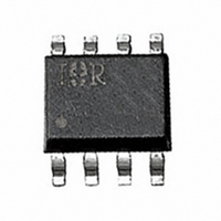
IPS042G International Rectifier, IPS042G Datasheet

IPS042G
Specifications of IPS042G
Available stocks
Related parts for IPS042G
IPS042G Summary of contents
Page 1
... Active clamp Low current & logic level input E.S.D protection Description The IPS042G is a fully protected dual low side SMART POWER MOSFET that features over-current, over-tem- perature, ESD protection and drain to source active clamp.This device combines a HEXFET ® POWER MOSFET and a gate driver. It offers full protection and high reliability required in harsh environments ...
Page 2
... IPS042G 31 Absolute Maximum Ratings Absolute maximum ratings indicate sustained limits beyond which damage to the device may occur. All voltage parameters are ref- erenced to SOURCE lead. (T Ambient = 25 copper thickness. Symbol Parameter V ds Maximum drain to source voltage V in Maximum input voltage I in, max ...
Page 3
... Min. Typ. Max. Units Test Conditions — 165 — 1.1 1.7 2.2 1.5 2 400 — — IPS042G 5V 14V 40V 20mA (see Fig.3 & shutdown (see Fig.3 & 50mA 14V over-current triggered See figure 2 s See figure 2 ...
Page 4
... IPS042G Functional Block Diagram All values are typical Lead Assignments 4 200 k 4000 > 165°c I > 1sd In1 S2 In2 8 Lead SOIC DRAIN sense SOURCE www.irf.com ...
Page 5
... Appl . Notes to evaluate power dissipation ) Figure 3 - Active clamp waveforms www.irf.com 90 % Vin 10 % Tr-in Tr-in t > T reset 90 % Ids Vds Figure rise time & switching time definitions T clamp Rem : V load is negative during demagnetization Figure 4 - Active clamp test circuit IPS042G Td off load + Vin IN Vds Ids 5 ...
Page 6
... IPS042G All curves are typical values with standard footprints. Operating in the shaded area is not recommended. 1200 1100 1000 900 800 700 600 500 400 300 200 100 Figure 5 - Rds Input Voltage (V) 10 ton delay 9 rise tim e 8 130% rdson Figure 7 - Turn-ON Delay Time, Rise Time & Time ...
Page 7
... Rds(on) (us Resistor ( ) 3 2.5 2 1.5 1 0.5 Isd 25°C Ilim 25° Figure 11 - Current Iim. & I shutdown (A) Vs Vin (V) www.irf.com 10000 Figure 10 - Turn-OFF Delay Time & Fall Time (us -50 - Figure shutdown (A) Vs Temperature ( IPS042G delay off fall tim Resistor ( ) 100 125 150 ...
Page 8
... IPS042G 3 Std. footprint 127°C/W m osfet on Std. footprint 100°C/W m osfet - 100 Figure 13 - Max.Cont. Ids ( Amb. Temperature ( C) 10 single pulse 1000 Hz rth=100°C/W dT=25°C 10kHz rth=100°C/W dT=25°C 1 Vbat = 14 V Tjini = T sd all curves for 1 mosfet active 0 Figure 15 - Iclamp (A) Vs Inductive Load (mH) ...
Page 9
... Figure 17 - Input current ( -50 - Figure 19 - Turn-on, Turn-off, and Treset ( www.irf.com 120% 115% 110% 105% 100% 95% 90% 85% 80% -50 - Treset rise tim e fall tim e 100 125 150 IPS042G Vds clam p @ Isd Vin clam p @ 10m 100 125 150 Figure 18 - Vin clamp and V clamp2 (%) ...
Page 10
... IPS042G 0.25 [.010 0.25 [.010 NOT ES: 1. DIMENSIONING & TOLE RANCING PE R ASME Y14.5M-1994. 2. CONTROLLING DIMENS ION: MILLIMET ER 3. DIMENSIONS ARE S HOWN IN MILLIME TE RS [INCHE S]. 4. OUT LINE CONFORMS T O JEDEC OUTLINE MS -012AA. IR WORLD HEADQUARTERS: 233 Kansas St., El Segundo, California 90245 Tel: (310) 252-7105 ...


