IPS5551T International Rectifier, IPS5551T Datasheet
IPS5551T
Specifications of IPS5551T
Available stocks


Related parts for IPS5551T

IPS5551T Summary of contents
Page 1
... Input referenced E.S.D protection Input referenced to Vcc Description The IPS5551T is a fully protected three terminal high side switch with built-in short-circuit, over-temperature, ESD protection, inductive load capability. The input signal is referenced to Vcc. When the input voltage Vcc - Vin is higher than the specified threshold, the output power MOSFET is turned on ...
Page 2
... IPS5551T Absolute Maximum Ratings Absolute maximum ratings indicate sustained limits beyond which damage to the device may occur. All voltage pa- rameters are referenced lead footprint with 70 m copper thickness Symbol Parameter max Maximum input voltage in1 max Max. transient Input voltage I in max ...
Page 3
... Min. Typ. Max. Units Test Conditions — 165 — 60 150 100 — 50 — IPS5551T I out =35A,Vcc -Vin=12V see Fig out =17A in out = 35A 150 C I out = 10mA I out = 35A - t < 100us 35A in out= A 12V 14V Vcc - Vin (note 2) ...
Page 4
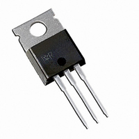
... IPS5551T Functional Block Diagram 10k 6mA + 4.7V 35V 4. Lead Assignments 4 Charge pump Level driver shift Over curren 100A - Tj + Over temperatur 165° (Vcc Vcc Out Super TO220 VCC 40V clamp VOUT www.irf.com ...
Page 5
... Vcc-Vout max Vclamp1 Vclamp2 Vcc 90% Iout Iout max -Ids cont. Vcc-Vout -Ids pulsed Iout 85° Isd Tr1 Figure 2 - Switching time definitions (turn-on) Vcc-Vin 12V 0 V Iout Isd Tj Tjsd Figure 4 - Protection timing diagram IPS5551T DV/dt(on) Tr2 t > T reset t < T reset OI shutdown OT shutdown 5 ...
Page 6
... IPS5551T Vcc - Vin Iout Iou Vclamp Vcc - Vout ( Vcc ) ( see Appl . Notes to evaluate power dissipation ) Figure 5 - Active clamp waveforms Figure 7 - Rds ( clamp Figure 6 - Rds(on) measurement schematic 200 150 100 Figure 8 - Normalized Rds (on) (%) POWER Measurement www.irf.com ...
Page 7
... Figure 10 - Iclamp (A) Vs Inductive Load ( H) 1000 100 10 125 150 Figure out (A) Vs Protection resp. Time (ms) IPS5551T single pulse 10 Hz rth=60°C/W dT=25°C 100Hz rth=60°C/W dT=25° Current path capability should be above this curve Load characteristic should be below this curve ° ...
Page 8
... IPS5551T 120 100 - 100 o Figure ( 100 Figure (mA ( 1E-05 1E-04 0.001 0.01 150 Figure 14 - Transient thermal impedance ( -50 - Free air 1inch² PCB Infinite heatsink 0 100 1000 o C/W) Vs Time ( 100 125 150 o Figure (mA www.irf.com ...
Page 9
... VIH 3 VIL Hysteresis -50 - 100 Figure threshold ( 100.00 I=Imax vs L (see fig.10) 10.00 30A I=10A 1.00 0.10 0.01 Figure (mJ) Vs Inductive load ( H) (Vcc = 14V, R load =0.5 ) www.irf.com 100 125 150 Figure on, E off (mJ out (A) IPS5551T Eon Eoff ...
Page 10
... IPS5551T DZ1 off System ground DZ1 optional additional voltage transient protection D2 : optional additional reverse battery protection See application note for details Figure 20 - Automotive typical connection Case outline Super TO220 11.00 [.433] A 10.00 [.394] 1.50 [.059] 0.50 [.020] 15.00 [.590] 14.00 [.552] ...