TC664EUNTR Microchip Technology, TC664EUNTR Datasheet - Page 16
TC664EUNTR
Manufacturer Part Number
TC664EUNTR
Description
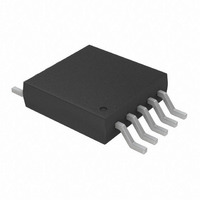
IC PWM FAN SPEED CONTRLR 10-MSOP
Manufacturer
Microchip Technology
Type
Controller - SMBus Fan Speedr
Datasheet
1.TC664EUN.pdf
(36 pages)
Specifications of TC664EUNTR
Applications
Fan Controller, Brushless (BLDC)
Number Of Outputs
1
Voltage - Supply
3 V ~ 5.5 V
Operating Temperature
-40°C ~ 85°C
Mounting Type
Surface Mount
Package / Case
10-MSOP, Micro10™, 10-uMAX, 10-uSOP
Product
Fan / Motor Controllers / Drivers
Operating Supply Voltage
3 V to 5.5 V
Supply Current
300 uA
Mounting Style
SMD/SMT
Lead Free Status / RoHS Status
Lead free / RoHS Compliant
Current - Output
-
Voltage - Load
-
Lead Free Status / Rohs Status
Lead free / RoHS Compliant
Available stocks
Company
Part Number
Manufacturer
Quantity
Price
Company:

Part Number:
TC664EUNTR
Manufacturer:
MICROCHIP
Quantity:
12 000


TC664/TC665
The data on the line must be changed during the LOW
period of the clock signal. There is one clock pulse per
bit of data. Each data transfer is initiated with a START
condition and terminated with a STOP condition. The
number of the data bytes transferred between the
START and STOP conditions is determined by the
master device and is unlimited.
5.1.7
Each receiving device, when addressed, is obliged to
generate an acknowledge bit after the reception of
each byte. The master device must generate an extra
clock pulse, which is associated with this acknowledge
bit.
The device that acknowledges has to pull down the
SDA line during the acknowledge clock pulse in such a
way that the SDA line is stable LOW during the HIGH
FIGURE 5-1:
FIGURE 5-2:
FIGURE 5-3:
DS21737A-page 16
S = Start Condition
P = Stop Condition
Shaded = Slave Transmission
S
S
S
S
Slave Address:
repeated due to change
in data flow direction.
ACKNOWLEDGE (ACK)
Slave Address
Slave Address
Slave Address
ADDRESS
ADDRESS
ADDRESS
ADDRESS
7 Bits
7 Bits
7 Bits
7 Bits
SMBus Protocol: Write Byte Format.
SMBus Protocol: Read Byte Format.
SMBus Protocol: Receive Byte Format.
WR
WR
RD
RD
ACK = Acknowledge = 0
NACK = Not Acknowledged = 1
WR = Write = 0
RD = Read = 1
ACK
ACK
ACK
ACK
Command Byte: selects
which register you are
writing to.
Command Byte: selects
which register you are
writing to.
Data Byte: reads from
the register set by the
command byte.
Data Byte: reads data from
the register commanded by
the last Read Byte or Write
Byte transmission
COMMAND
COMMAND
8 Bits
8 Bits
DATA
8 Bits
DATA
8 Bits
period of the acknowledge related clock pulse. Setup
and hold times must be taken into account. During
reads, a master device must signal an end of data to
the slave by not generating an acknowledge bit on the
last byte that has been clocked out of the slave. In this
case, the slave (TC664/TC665) will leave the data line
HIGH to enable the master device to generate the
STOP condition.
5.2
The TC664/TC665 devices communicate with three
standard SMBus protocols. These are the write byte,
read byte and receive byte. The receive byte is a short-
ened method for reading from or writing to a register
which had been selected by the previous read or write
command. These transmission protocols are shown in
Figures 5-1, 5-2 and 5-3.
NACK
NACK
ACK
ACK
SMBus Protocols
Data Byte: data goes
into the register set
by the command byte.
DATA
8 Bits
P
P
2002 Microchip Technology Inc.
ACK
P
Related parts for TC664EUNTR
Image
Part Number
Description
Manufacturer
Datasheet
Request
R

Part Number:
Description:
Manufacturer:
Microchip Technology Inc.
Datasheet:
Part Number:
Description:
Manufacturer:
Microchip Technology Inc.
Datasheet:
Part Number:
Description:
Manufacturer:
Microchip Technology Inc.
Datasheet:
Part Number:
Description:
Manufacturer:
Microchip Technology Inc.
Datasheet:
Part Number:
Description:
Manufacturer:
Microchip Technology Inc.
Datasheet:
Part Number:
Description:
Manufacturer:
Microchip Technology Inc.
Datasheet:
Part Number:
Description:
Manufacturer:
Microchip Technology Inc.
Datasheet:
Part Number:
Description:
Manufacturer:
Microchip Technology Inc.
Datasheet: