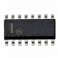
CS7054YDWR16 ON Semiconductor, CS7054YDWR16 Datasheet

CS7054YDWR16
Specifications of CS7054YDWR16
Related parts for CS7054YDWR16
CS7054YDWR16 Summary of contents
Page 1
... OSC R OSC CTL NC NC SO–16L A = Assembly Location WL Wafer Lot YY Year WW Work Week ORDERING INFORMATION Device Package CS7054YN14 CS7054YDW16 SO–16L CS7054YDWR16 SO–16L 1000 Tape & Reel 1 DIP–14 N SUFFIX CASE 646 SO–16L DW SUFFIX CASE 751G PGND INH I ADJ I SENSE+ I SENSE– V REG ...
Page 2
H V BAT 1000 F PWM Input ABSOLUTE MAXIMUM RATINGS* Storage Temperature V CC Supply Voltage Range (Load Dump = 26 V w/Series 51 Input Voltage Range (at any input) Maximum Junction Temperature ESD Susceptibility ...
Page 3
ELECTRICAL CHARACTERISTICS Characteristic V Supply CC Operating Current Supply Quiescent Current Overvoltage Shutdown Overvoltage Hysteresis Control (CTL) Control Input Current Sleep Mode Threshold Sleep Mode Hysteresis Current Sense Differential Voltage Sense I Input Current ADJ Linear Regulator Output Voltage Inhibit ...
Page 4
PACKAGE PIN # DIP–14 SO–16L 5.0 V Regulator REG ...
Page 5
TYPICAL PERFORMANCE CHARACTERISTICS 5.04 5.02 2.0 mA 5.00 4.98 4.96 4.94 – Temperature Figure 3. V vs. Temperature @ V REG 5.04 2.0 mA 5.02 5.00 4.98 4.96 4.94 – Temperature Figure 5. V vs. Temperature ...
Page 6
... Voltage Duty Cycle Conversion The IC translates an input voltage at the CTL lead into a duty cycle at the OUTPUT lead. The transfer function incorporates ON Semiconductor’s patented Voltage Compensation method to keep the average voltage and current across the load constant regardless of fluctuations in the supply voltage. The duty cycle is varied based upon the input voltage and supply voltage by the following equation: 2 ...
Page 7
Both leads source 50 A while the chip is in run mode. R should be much less than 1000 CS to minimize error in the I equation. I ...
Page 8
CS7054 10 V BAT kHz 150 Hz 5 MCU 100 k 100 100 k Figure 9. Frequency Converter http://onsemi.com OUTPUT V CC ...
Page 9
–T– 16X e 14X T PACKAGE THERMAL DATA Parameter CS7054 PACKAGE DIMENSIONS DIP–14 N SUFFIX CASE 646–04 ISSUE ...
Page 10
Notes CS7054 http://onsemi.com 10 ...
Page 11
Notes CS7054 http://onsemi.com 11 ...
Page 12
... CENTRAL/SOUTH AMERICA: Spanish Phone: 303–308–7143 (Mon–Fri 8:00am to 5:00pm MST) Email: ONlit–spanish@hibbertco.com ASIA/PACIFIC: LDC for ON Semiconductor – Asia Support Phone: 303–675–2121 (Tue–Fri 9:00am to 1:00pm, Hong Kong Time) Toll Free from Hong Kong & Singapore: 001–800–4422–3781 Email: ONlit– ...


