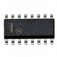
MC33030DWR2G ON Semiconductor, MC33030DWR2G Datasheet - Page 4

MC33030DWR2G
Manufacturer Part Number
MC33030DWR2G
Description
IC CTRLR/DRVR DC SERVO 16-SOIC
Manufacturer
ON Semiconductor
Type
DC Motor Driverr
Datasheet
1.MC33030P.pdf
(17 pages)
Specifications of MC33030DWR2G
Applications
DC Motor Controller, Servo
Number Of Outputs
1
Current - Output
1A
Voltage - Supply
8 V ~ 36 V
Operating Temperature
-40°C ~ 85°C
Mounting Type
Surface Mount
Package / Case
16-SOIC (0.300", 7.5mm Width)
Supply Current
25 mA
Mounting Style
SMD/SMT
Lead Free Status / RoHS Status
Lead free / RoHS Compliant
Voltage - Load
-
Lead Free Status / Rohs Status
Lead free / RoHS Compliant
Available stocks
Company
Part Number
Manufacturer
Quantity
Price
Company:
Part Number:
MC33030DWR2G
Manufacturer:
MICROCHIP
Quantity:
1 000
3. The upper or lower hysteresis will be lost when operating the Input, Pin 3, close to the respective rail. Refer to Figure 4.
4. Low duty cycle pulse techniques are used during test to maintain junction temperature as close to ambient temperature as possible.
ELECTRICAL CHARACTERISTICS
WINDOW DETECTOR
OVERCURRENT MONITOR
POWER H−SWITCH
TOTAL DEVICE
Input Hysteresis Voltage (V
Input Dead Zone Range (V
Input Offset Voltage ( ⎢[V
Input Functional Common−Mode Range (Note 3)
Reference Input Self Centering Voltage
Window Detector Propagation Delay
Overcurrent Reference Resistor Voltage (Pin 15)
Delay Pin Source Current
Delay Pin Sink Current (R
Delay Pin Voltage, Low State (I
Overcurrent Shutdown Threshold
Overcurrent Shutdown Propagation Delay
Drive−Output Saturation (− 40°C p T
Drive−Output Voltage Switching Time (C
Brake Diode Forward Voltage Drop (I
Standby Supply Current
Overvoltage Shutdown Threshold
Overvoltage Shutdown Hysteresis (Device “off” to “on”)
Operating Voltage Lower Threshold
Upper Threshold
Lower Threshold
Pins 1 and 2 Open
Comparator Input, Pin 3, to Drive Outputs
V
V
V
V
V
V
V
Delay Capacitor Input, Pin 16, to Drive Outputs, V
High−State
Low−State
Rise Time
Fall Time
ID
DLY
DLY
DLY
DLY
CC
CC
= 0.5 V, R
= 14 V
= 8.0 V
= 0 V, R
= 5.0 V
= 8.3 V
= 14 V
OC
L(DRV)
= 27 k, I
= 390 W
2
− V
OC
2
1
Characteristic
− V
DRV
− V
Pin 2
= 27 k, I
DLY
4
4
, Figure 18)
= 0 mA
, V
] − [V
= 0 mA)
2
F
DRV
A
− V
Pin 2
= 200 mA, Note 4)
p+ 85°C, Note 4)
L
(continued) (V
3
= 0 mA)
= 15 pF)
, Figure 18)
− V
(− 40°C p T
(− 40°C p T
4
] ⎟ Figure 18)
(I
ID
source
(I
CC
= 0.5 V
sink
http://onsemi.com
A
A
= 14 V, T
p + 85°C)
p + 85°C)
= 100 mA)
= 100 mA)
MC33030
4
A
= 25°C, unless otherwise noted.)
I
t
DLY(source)
p(DLY/DRV)
V
t
V
V
I
Symbol
p(IN/DRV)
DLY(sink)
V
V
V
OH(DRV)
OL(DRV)
OL(DLY)
V
V
R
th(OC)
V
th(OV)
H(OV)
V
V
I
V
V
V
RSC
CC
IDZ
t
OC
t
CC
IO
IH
IL
r
f
H
F
(V
CC
16.5
Min
166
3.9
6.8
5.5
0.3
25
−
−
−
−
−
−
−
−
−
−
−
−
−
−
−
−
−
− 2)
(V
(V
(1/2 V
CC
CC
0.24
16.5
0.12
1.04
Typ
210
200
200
2.0
4.3
5.5
0.1
0.7
0.3
7.5
6.0
1.8
0.6
7.5
35
25
14
18
− 1.05)
− 0.85)
CC
)
Max
20.5
254
4.7
6.9
0.4
8.2
6.5
1.0
2.5
1.0
8.0
45
25
−
−
−
−
−
−
−
−
−
−
−
−
Unit
mV
mV
mV
mA
mA
mA
ms
ms
ns
V
V
V
V
V
V
V
V
V
V


