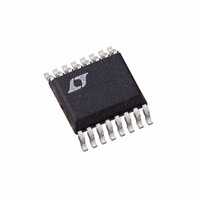
LTC1473CGN Linear Technology, LTC1473CGN Datasheet - Page 10

LTC1473CGN
Manufacturer Part Number
LTC1473CGN
Description
IC SWITCH DVR PWRPATH DUAL16SSOP
Manufacturer
Linear Technology
Series
PowerPath™r
Datasheet
1.LTC1473CGNPBF.pdf
(16 pages)
Specifications of LTC1473CGN
Applications
Handheld/Mobile Devices
Fet Type
N-Channel
Number Of Outputs
2
Internal Switch(s)
No
Delay Time - On
22µs
Delay Time - Off
1µs
Voltage - Supply
4.75 V ~ 30 V
Current - Supply
100µA
Operating Temperature
0°C ~ 70°C
Mounting Type
Surface Mount
Package / Case
16-SSOP
Lead Free Status / RoHS Status
Contains lead / RoHS non-compliant
Available stocks
Company
Part Number
Manufacturer
Quantity
Price
Part Number:
LTC1473CGN
Manufacturer:
LINEAR/凌特
Quantity:
20 000
APPLICATIONS
LTC1473
As a general rule, select the switch with the lowest R
and able to withstand the maximum allowable V
will minimize the heat dissipated in the switches while
increasing the overall system efficiency. Higher switch
resistances can be tolerated in some systems with lower
current requirements, but care should be taken to ensure
that the power dissipated in the switches is never allowed
to rise above the manufacturers’ recommended level.
Inrush Current Sense Resistor, R
A small valued sense resistor (current shunt) is used by
the two switch pair drivers to measure and limit the inrush
or short-circuit current flowing through the conducting
switch pair.
The inrush current limit should be set at approximately 2
or 3 the maximum required output current. For example,
if the maximum current required by the DC/DC converter
is 2A, an inrush current limit of 6A is set by selecting a
0.033 sense resistor, R
mula:
Note that the voltage drop across the resistor in this
example is only 66mV under normal operating conditions.
Therefore, the power dissipated in the resistor is ex-
tremely small (132mW), and a small 1/4W surface mount
resistor can be used in this application (the resistor will
tolerate the higher power dissipation during current limit
for the duration of the fault time-out). A number of small
valued surface mount resistors are available that have
been specifically designed for high efficiency current
sensing applications.
Programmable Fault Timer Capacitor, C
A fault timer capacitor, C
duration the MOSFET switches are allowed to be in con-
tinuous current limit.
In the event of a fault condition, the MOSFET switch is
driven into current limit by the inrush current limit loop.
The MOSFET switch operating in current limit is in a high
dissipation mode and can fail catastrophically if not
promptly terminated.
10
R
SENSE
= (200mV)/I
U
INRUSH
TIMER
INFORMATION
SENSE
U
, is used to program the time
, using the following for-
SENSE
W
TIMER
U
DS
DS(ON)
. This
The fault time delay is programmed with an external
capacitor between the TIMER pin and GND. At the instant
the MOSFET switch enters current limit, a 5.5 A current
source starts charging C
When the voltage across C
latch is set and the MOSFET switch is turned off. To reset
the latch, the logic input of the MOSFET gate driver is
deselected.
The fault time delay should be programmed as large as
possible, at least 3 to 5 the maximum switching transi-
tion period, to avoid prematurely tripping the protection
circuit. Conversely, for the protection circuit to be effec-
tive, the fault time delay must be within the safe operating
area of the MOSFET switches, as stated in the
manufacturer’s data sheet.
The maximum switching transition period happens during
a cold start, when a fully charged battery is connected to
an unpowered system. The inrush current charging the
system supply capacitor to the battery voltage determines
the switching transition period.
The following example illustrates the calculation of C
Assume the maximum battery voltage is 20V, the system
supply capacitor is 68 F, the inrush current limit is 6A and
the maximum current required by the DC/DC converter is
2A. Then, the maximum switching transition period is
calculated using the following formula:
Multiplying 3 by 340 s gives 1.02ms, the minimum fault
delay time. Make sure this delay time does not fall outside
of the safe operating area of the MOSFET switch dissipat-
ing 60W (6A • 20V/2). Using this delay time the C
be calculated using the following formula:
Therefore, C
t
t
C
SW(MAX)
SW(MAX)
TIMER
= 1.02ms
TIMER
=
=
(V
(20)(68 F)
BAT(MAX)
6A – 2A
should be 4700pF.
I
INRUSH
5.5 A
1.20V
TIMER
TIMER
)(C
– I
= 340 s
= 4700pF
IN(DC/DC)
LOAD
through the TIMER pin.
reaches 1.2V an internal
)
TIMER
TIMER.
can


