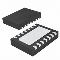
LTC4355IDE#PBF Linear Technology, LTC4355IDE#PBF Datasheet - Page 3

LTC4355IDE#PBF
Manufacturer Part Number
LTC4355IDE#PBF
Description
IC IDEAL DIODE-OR 14-DFN
Manufacturer
Linear Technology
Datasheet
1.LTC4355ISPBF.pdf
(20 pages)
Specifications of LTC4355IDE#PBF
Applications
-48V Dist Power Systems, AdvancedTCA ® Systems
Fet Type
N-Channel
Number Of Outputs
2
Internal Switch(s)
No
Delay Time - Off
300ns
Voltage - Supply
9 V ~ 80 V
Current - Supply
2mA
Operating Temperature
-40°C ~ 85°C
Mounting Type
Surface Mount
Package / Case
14-DFN
Lead Free Status / RoHS Status
Lead free / RoHS Compliant
Delay Time - On
-
Available stocks
Company
Part Number
Manufacturer
Quantity
Price
ELECTRICAL CHARACTERISTICS
temperature range, otherwise specifi cations are at T
SYMBOL
V
I
I
ΔV
I
I
t
V
V
I
V
V
ΔV
ΔV
ΔV
V
I
R
R
R
Note 1: Stresses beyond those listed under Absolute Maximum Ratings
may cause permanent damage to the device. Exposure to any Absolute
Maximum Rating condition for extended periods may affect device
reliability and lifetime.
OUT
INx
GATEx(UP)
GATEx(DN)
OFF
MONx(IN)
FLT
OUT
MONx(TH)
MONx(HYST)
INx(TH)
INx(HYST)
FLT
SET(L)
SET(M)
SET(H)
GATEx
SD
SD(FLT)
SD(FLT)(HYST)
PARAMETER
Operating Supply Range
Supply Current
INx Pin Input Current
External N-Channel Gate Drive
(V
External N-Channel Gate Pull-Up Current
External N-Channel Gate Pull-Down in Fault
Condition
Gate Turn-Off Time
MONx Pin Threshold Voltage
MONx Pin Hysteresis Voltage
MONx Pin Input Current
INx Pin Threshold Voltage
INx Pin Hysteresis Voltage
Source-Drain Regulation Voltage
(V
Short-Circuit Fault Voltage
(V
Short-Circuit Fault Hysteresis Voltage
PWRFLTx, FUSEFLTx, VDSFLT Pins
Output Low
PWRFLTx, FUSEFLTx, VDSFLT Pins
Leakage Current
SET Resistance Range for ΔV
SET Resistance Range for ΔV
SET Resistance Range for ΔV
GATEx
INx
INx
– V
– V
– V
OUT )
OUT
INx
) Rising
)
SD(FLT)
SD(FLT)
SD(FLT)
= 0.25V
= 0.5V
= 1.5V
A
= 25°C. 9V < V
CONDITIONS
GATE High
V
V
V
V
Gate Drive Off, V
V
V
V
V
V
V
SET = 0V
SET = 100kΩ
SET = Hi-Z
I
V
PWRFLTx
OUT
OUT
GATEx
INx
INx
GATEx
MONx
MONx
INx
GATEx
PWRFLTx
The
– V
– V
Rising
= 20V to 80V
= 9V to 20V
Rising
= 1.23V
= V
– V
– V
l
OUT
OUT
, I
, V
denotes the specifi cations which apply over the full operating
FUSEFLTx
INx
INx
INx
FUSEFLTx
= 55mV
= 100mV
,
< 1V
= 2.5V
OUT
Note 2: All currents into pins are positive, all voltages are referenced to
GND unless otherwise specifi ed.
Note 3: The GATEx pins are internally limited to a minimum of 13V above
INx. Driving these pins beyond the clamp may damage the part.
GATEx
, I
< 80V, unless otherwise noted.
, V
–
VDSFLT
|
–
–1V, C
VDSFLT
= V
INx
= 5mA
GATE
+5V
= 5V
= 0
l
l
l
l
l
l
l
l
l
l
l
l
l
l
l
l
l
l
l
l
l
l
1.209
MIN
–14
0.5
4.5
0.2
0.4
1.3
10
10
25
10
50
9
1
3
0
1
1.227
0.25
TYP
–20
100
0.6
0.3
3.5
0.5
1.5
14
30
75
25
30
2
6
2
0
0
LTC4355
1.245
MAX
–26
150
200
150
1.2
0.4
0.3
0.6
1.6
80
18
18
45
±1
55
±1
3
4
5
UNITS
4355fe
3
MΩ
mA
mA
mV
mV
mV
mV
mV
kΩ
kΩ
μA
μA
μA
μs
V
V
V
A
V
V
V
V
V


