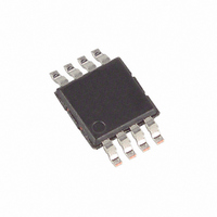
MAX8535EUA+T Maxim Integrated Products, MAX8535EUA+T Datasheet - Page 12

MAX8535EUA+T
Manufacturer Part Number
MAX8535EUA+T
Description
IC CNTRLR ORING MOSFET 8-MSOP
Manufacturer
Maxim Integrated Products
Datasheet
1.MAX8535EUA.pdf
(20 pages)
Specifications of MAX8535EUA+T
Applications
Network/Telecom Power Supplies, Rectifiers
Fet Type
N-Channel
Number Of Outputs
1
Internal Switch(s)
No
Delay Time - Off
200ns
Voltage - Supply
8 V ~ 14 V
Current - Supply
2mA
Operating Temperature
-40°C ~ 85°C
Mounting Type
Surface Mount
Package / Case
8-MSOP, Micro8™, 8-uMAX, 8-uSOP,
Lead Free Status / RoHS Status
Lead free / RoHS Compliant
Delay Time - On
-
Lead Free Status / Rohs Status
Lead free / RoHS Compliant
ORing MOSFET Controllers with Fastest
Fault Isolation for Redundant Power Supplies
Critical loads often employ parallel-connected power
supplies with redundancy to enhance system reliability.
The MAX8535/MAX8536/MAX8585 are highly integrated
but inexpensive MOSFET controllers that provide isolation
and redundant power capability in high-reliability sys-
tems. The MAX8535/MAX8585 is used in 12V systems
and has an internal charge pump to drive the gates of the
n-channel pass elements to V
used in 3.3V and 5V systems, with a charge pump output
of V
During startup, the MAX8535/MAX8536/MAX8585 moni-
tor the voltage drop across external MOSFETs. Once
V
MOSFETs are turned on. The MAX8535/MAX8536/
MAX8585 feature a dual-purpose TIMER input. A single
external resistor from TIMER to ground sets the turn-on
speed of the external MOSFETs. Optionally, the TIMER
input can be used as a logic-enable pin. Once the
device is turned on, the MAX8535/MAX8536/MAX8585
monitor the load, protecting against overvoltage, under-
voltage, and reverse-current conditions.
Overvoltage and undervoltage fault thresholds are
adjustable and can be disabled. The current-limit trip
points are set by the external MOSFETs’ R
reducing component count. An open-drain logic-low
fault output indicates if an overvoltage, undervoltage, or
reverse-current fault occurs.
12
CC
CC
______________________________________________________________________________________
PIN
approaches or exceeds the bus voltage, the
1
2
3
4
5
6
7
8
+ 5V.
FAULT
NAME
TIMER
GATE
GND
UVP
OVP
V
CS
CC
Detailed Description
Gate Drive Output. Bypass GATE with a 0.01µF capacitor to ground.
Ground
Power-Supply Input. Bypass V
Undervoltage Input. Connect a resistor-divider from the V
to UVP. Leave high impedance if not used. UVP fault threshold must be set above V
Timer Input. Connect a resistor from TIMER to ground to select the charge-pump operating
frequency. The charge-pump frequency is proportional to the TIMER output current. TIMER can
source up to 100µA. If pulled low (<0.5V), the gate drive is disabled. If pulled high (above 1.25V), the
charge pump operates at 550kHz.
Overvoltage Input. Connect a resistor-divider from the CS to GND with the center point connected to
OVP. Connect to GND if not used.
Open-Drain Fault Output. FAULT is low during a fault, high impedance during normal operation.
Connect a pullup resistor of 50k or higher value to a voltage rail.
Current-Sensing Input. Connect CS to the positive side of the system bus. Bypass with 1nF capacitor
to GND.
CC
+ 10V. The MAX8536 is
DS(ON)
CC
,
with a 0.1µF capacitor to ground.
V
MAX8536/MAX8585 and the input to the internal charge
pump that drives the gate of the external MOSFETs. The
MAX8535/MAX8536/MAX8585 monitor V
V
DC-DC power modules). During startup, the device
turns on when V
old V
greater than (CS - 0.4V), the charge pump turns on, dri-
ving GATE high and turning on the external MOSFETs.
The MAX8535/MAX8536/MAX8585 provide a program-
mable-frequency charge pump and shutdown function
through TIMER. Slowing down the charge-pump fre-
quency allows a user to program soft-start. Connecting
a resistor from TIMER to GND sets the charge-pump fre-
quency from 100kHz to 500kHz. Connecting TIMER to a
logic high sets charge-pump operation to a maximum
frequency of 550kHz. Pulling TIMER to GND shuts down
the charge pump and turns off the external MOSFET.
Reducing the charge-pump frequency increases the
I
Fault section).
GATE is the output of the internal charge pump that
drives the external MOSFETS. During startup, the GATE
voltage ramps up according to the charge-pump fre-
quency. At 250kHz, the GATE drive current for the
MAX8535/MAX8585 is 25µA and the GATE drive current
REVERSE
CC
CC
connects directly to the power supply (Silver Box or
FUNCTION
is the power-supply input for the MAX8535/
CCOK
startup blank time (see the Reverse-Current
. After V
CC
CC
to GND with the center point connected
rises above the undervoltage thresh-
CC
exceeds V
Pin Description
CCOK
CCOK
CC
and V
threshold.
at all times.
TIMER
GATE
CC
V
CC
is


