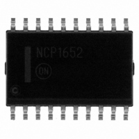
NCP1652DWR2G ON Semiconductor, NCP1652DWR2G Datasheet - Page 27

NCP1652DWR2G
Manufacturer Part Number
NCP1652DWR2G
Description
IC PFC CONTROLLER CCM/DCM 20SOIC
Manufacturer
ON Semiconductor
Datasheet
1.NCP1652DR2G.pdf
(34 pages)
Specifications of NCP1652DWR2G
Mode
Continuous Conduction (CCM), Discontinuous Conduction (DCM)
Frequency - Switching
100kHz
Current - Startup
5.62mA
Voltage - Supply
9.3 V ~ 20 V
Operating Temperature
-40°C ~ 125°C
Mounting Type
Surface Mount
Package / Case
20-SOIC (7.5mm Width)
Switching Frequency
20 KHz to 250 KHz
Maximum Operating Temperature
+ 125 C
Mounting Style
SMD/SMT
Minimum Operating Temperature
- 40 C
Lead Free Status / RoHS Status
Lead free / RoHS Compliant
Other names
NCP1652DWR2GOSTR
Output Overload
output power of the converter. An internal 6.7 kW resistor
pulls−up the FB voltage to the internal 6.5 V reference. An
external optocoupler pulls down the FB voltage to regulate
the output voltage of the system. The optocoupler is off
during power up and output overload conditions allowing
the FB voltage to reach its maximum level.
overload condition. A typical startup time of a single PFC
stage converter is around 100 ms. If the converter is out of
regulation (FB voltage exceeds 5.0 V) for more that 150 ms
(typical) the drivers are disabled and the controller enters the
double hiccup mode to reduce the average power
dissipation. A new startup sequence is initiated after the
double hiccup is complete. This protection feature is critical
to reduce power during an output short condition.
Soft−Skip™ Cycle Mode
converter reduces. Once V
threshold, V
The skip comparator hysteresis is typically 180 mV.
additional output power is delivered. As the output voltage
decreases the feedback voltage increases to maintain the
output voltage in regulation. This mode of operation is
known as skip mode. The skip mode frequency is dependent
of load loop gain and output capacitance and can create
audible noise due to mechanical resonance in the
transformer and snubber capacitor. A proprietary
Soft−Skip™ mode reduces audible noise by slowly
increasing the primary peak current until it reaches its
maximum value. The minimum skip ramp period, t
2.5 ms. Figure 65 shows the relationship between V
V
The NCP1652 disables Soft−Skip™ when the rectified ac
line voltage drops to its valley level. This ensures the
primary current always ramp up reducing audible noise. A
skip event occurring as the ac line voltage is decreasing,
causes the primary peak current to ramp down instead of
ramp up. Once the skip period is over the primary current is
only determined by the ac line voltage. A Soft−Skip™ event
terminates once the AC−IN pin voltage decreases below
SSKIP
The Feedback Voltage, V
The NCP1652 monitors the FB voltage to detect an
The FB voltage reduces as the output power demand of the
The converter output voltage starts to decay because no
Skip mode operation is synchronous of the ac line voltage.
and the primary current.
Figure 65. Soft−Skip] operation.
SSKIP
, 1.30 V (typical) the drivers are disabled.
FB
, is directly proportional to the
FB
drops below the skip
SSKIP
http://onsemi.com
FB
, is
,
27
260 mV. A new Soft−Skip™ period starts once the voltage
on the AC−IN pin increases to 260 mV.
Soft−Skip™ event. A transient load detector terminates a
Soft−Skip™ period once V
more than 550 mV. This ensures the required output power
is delivered during a load transient and the output voltage
does not fall out of regulation. Figure 66 shows the
relationship between Soft−Skip™ and the transient load
detector.
the PWM Comparator output to control the duty ratio. The
Soft−Skip™ Comparator controls the duty ratio in skip
mode and the PWM Comparator controls the duty cycle
during normal operation. In skip mode, the non−inverting
input of the Soft−Skip™ Comparator exceeds 4 V, disabling
the drivers. As the FB voltage increases, the voltage at the
non−inverting input is ramp down from 4 V to 0.2 V to
enable the drivers.
Multiplier and Reference Generator
output power of the converter. This controller uses a
proprietary concept for the multiplier used within the
reference generator. This innovative design allows greatly
improved accuracy compared to a conventional linear
analog multiplier. The multiplier uses a PWM switching
circuit to create a scalable output signal, with a very well
defined gain.
ac-reference signal is used to shape the input current. The
multiplier has three inputs, the error signal from an external
error amplifier (V
(AC_IN) and the feedforward input (V
applied to the V
circuit. The FB voltage is converted to a current with a V-I
An increase in output load current terminates a
The output of the Soft−Skip™ Comparator is or−ed with
The NCP1652 uses a multiplier to regulate the average
The output of the multiplier is the ac-reference signal. The
The FB signal from an external error amplifier circuit is
Figure 66. Load transient during Soft−Skip]
V
FB
FB
pin via an optocoupler or other isolation
FB
V
SSKIP
), the full wave rectified ac input
FB
voltage exceeds V
FF
).
SSKIP
by


