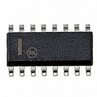
NCP1650DR2 ON Semiconductor, NCP1650DR2 Datasheet - Page 29

NCP1650DR2
Manufacturer Part Number
NCP1650DR2
Description
IC CTRLR PWR FACTOR PWM 16SOIC
Manufacturer
ON Semiconductor
Datasheet
1.NCP1650DR2G.pdf
(31 pages)
Specifications of NCP1650DR2
Mode
Continuous Conduction (CCM), Discontinuous Conduction (DCM)
Frequency - Switching
100kHz
Voltage - Supply
10 V ~ 20 V
Operating Temperature
-40°C ~ 125°C
Mounting Type
Surface Mount
Package / Case
16-SOIC (3.9mm Width)
Switching Frequency
25 KHz to 250 KHz
Maximum Operating Temperature
+ 125 C
Mounting Style
SMD/SMT
Minimum Operating Temperature
- 40 C
Lead Free Status / RoHS Status
Contains lead / RoHS non-compliant
Current - Startup
-
Lead Free Status / Rohs Status
Lead free / RoHS Compliant
Other names
NCP1650DR2OSTR
Available stocks
Company
Part Number
Manufacturer
Quantity
Price
Part Number:
NCP1650DR2G
Manufacturer:
ON/安森美
Quantity:
20 000
Power Loop
Block Diagram
down into four sections. These are the power multiplier,
power amplifier, reference signal and modulator and output
stage.
circuitry has been greatly simplified due to the location of
the associated poles and zeros.
on the power multiplier and the second is due to the power
error amplifier. Because the pole on the power multiplier is
very low, it will normally be necessary to include the resistor
(R
V
line
V pm
V ac =
f p =
The block diagram for the power loop has been broken
Similar to the voltage loop, the modulator and output stage
There are two significant poles in this circuit. The first is
C
8
i
R
R
9
) for the zero on this amplifier.
o
ac1
ac2
POWER MULTIPLIER
AC INPUT
=
R
2 π C 9 R 9
P
9
max
R ac1 + R ac2
3.75 R 9 V ac R S
V line R ac2
5
9
1
V
ac
R 10
MULTIPLIER
POWER
2.5 V
(High Frequency Gain, Past Zero)
V
pm
A v =
f z =
A v = G m R 8
POWER AMP
+
--
LOOP COMP
POWER
2 π C 8 R 8
AMP
2 π f C 8
V
G m
pa
1
R
8
C
8
8
Figure 45. Power Loop Model
ORing NET
--0.32 mA/V
REFERENCE SIGNAL
http://onsemi.com
V ref
V ac =
V pa
= --2 V ac
29
R ac1 + R ac2
REFERENCE
MULTIPLIER
V line R ac2
Power Multiplier
voltage. This multiplier has a very low frequency pole that
must be considerably lower than the line frequency, so that
the power signal is essentially a DC level.
Reference Signal
loop model.
Modulator and Output Stage
modulator and output circuitry follows the path from the AC
reference voltage (Vref) to the output current. Since this
circuit regulates the power, and the input and output voltages
are the two basic components of the power, the output
current is the output variable for this block.
The power multiplier’s gain is a function of the input
The reference signal block is unchanged from the voltage
For the power circuit, the transfer function of the
There is no pole associated with this function.
25 k
V
ref
ERROR
AMP
AC
+
--
MODULATOR AND OUTPUT STAGE
4 V
I
C.S. Amp
avg
--
+
V ref
i
o
PWM
10
R
10
=
225k R S
LOGIC
R 10
OUT
16
12
I
S--
I
R
Q1
O
S


