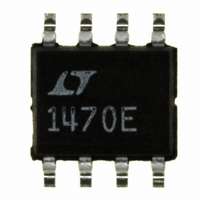
LTC1470ES8#PBF Linear Technology, LTC1470ES8#PBF Datasheet - Page 5

LTC1470ES8#PBF
Manufacturer Part Number
LTC1470ES8#PBF
Description
IC SWTCH PCMCIA3.3V/5V SNGL8SOIC
Manufacturer
Linear Technology
Type
PCMCIA/Cardbus Switchr
Datasheet
1.LTC1470CS8PBF.pdf
(12 pages)
Specifications of LTC1470ES8#PBF
Number Of Outputs
1
Rds (on)
180 mOhm
Internal Switch(s)
Yes
Current Limit
1A
Voltage - Input
3.3V, 5V
Operating Temperature
-40°C ~ 85°C
Mounting Type
Surface Mount
Package / Case
8-SOIC (3.9mm Width)
Lead Free Status / RoHS Status
Lead free / RoHS Compliant
Available stocks
Company
Part Number
Manufacturer
Quantity
Price
BLOCK
PIN
LTC1471
AOUT, BOUT(Pins 1, 16, 8, 9): Output Pins. The outputs
of the LTC1471 are switched between three operating
states: OFF, 3.3V and 5V. These pins are protected against
accidental short circuits to ground by SafeSlot current
limit circuitry which protects the socket, the card, and the
system power supplies against damage. A second level of
protection is provided by thermal shutdown circuitry.
5V
pins serve two purposes. The first purpose is as the power
supply input for the 5V NMOS switches. The second
purpose is to provide power for the input, gate drive, and
protection circuitry. These pins must therefore be con-
tinuously powered.
EN1, EN0 (Pins 3, 4, 11, 12): Enable Inputs. The enable
inputs are designed to interface directly with industry
standard PCMCIA controllers and are high impedance
CMOS gates with ESD protection diodes to ground, and
IN
U
(Pins 2, 10): 5V Input Supply Pins. The 5V
FUNCTIONS
EN0
EN1
U
DIAGRAM
TTL-TO-CMOS
TTL-TO-CMOS
CONVERTER
CONVERTER
U
W
(LTC1470 or 1/2 LTC1471)
BREAK-BEFORE-
MAKE SWITCH
AND CONTROL
IN
supply
OSCILLATOR
AND BIAS
should not be forced above 5V
inputs have about 100mV of built-in hysteresis to ensure
clean switching between operating modes. The LTC1471
is designed to operate without 12V power. The gates of the
V
the 5V
for more detail). The enable inputs should be turned off at
least 100µs before the 5V
that all NMOS switch gates are fully discharged and are in
the high impedance mode.
GND (Pins 5, 13): Ground Connections.
3V
supply pins serve as the power supply input for the 3.3V
switches. These pins do not not provide any power to the
internal control circuitry, and therefore, do not consume
any power when unloaded or turned off.
CC
IN
NMOS switches are powered by charge pumps from
(Pins 6, 7, 14, 15): 3V Input Supply Pins. The 3V
IN
supply pins (see Applications Information section
CONTROL LOGIC
CONTROL LOGIC
GATE CHARGE
GATE CHARGE
DISCHARGE
DISCHARGE
CHARGE
PUMP
AND
AND
LTC1470/LTC1471
CURRENT LIMIT
IN
AND THERMAL
SHUTDOWN
power is removed to ensure
IN
or below ground. All four
0.14Ω
0.12Ω
5V
OUTPUT
3V
LTC1470-BD01
IN
IN
14701fa
5
IN


