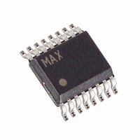
MAX1602EEE+ Maxim Integrated Products, MAX1602EEE+ Datasheet - Page 2

MAX1602EEE+
Manufacturer Part Number
MAX1602EEE+
Description
IC CARDBUS SNGL & PCMCIA 16-QSOP
Manufacturer
Maxim Integrated Products
Datasheet
1.MAX1602EEE.pdf
(12 pages)
Specifications of MAX1602EEE+
Applications
Processor
Operating Temperature
-40°C ~ 85°C
Mounting Type
Surface Mount
Package / Case
16-QSOP
Output Voltage Range
0.4 V
Output Current
260 mA
Input Voltage Range
3 V to 5.5 V
Input Current
20 uA
Power Dissipation
667 mW
Operating Temperature Range
- 40 C to + 85 C
Mounting Style
SMD/SMT
Lead Free Status / RoHS Status
Lead free / RoHS Compliant
Current - Supply
-
Voltage - Supply
-
Lead Free Status / Rohs Status
Lead free / RoHS Compliant
ABSOLUTE MAXIMUM RATINGS
Inputs/Outputs to GND
VPP Input/Output to GND
Logic Inputs to GND (A0VCC, A1VCC,
CODE Input to GND ........................................-0.3V, (VY + 0.3V)
VCC Output Current (Note 2)...................................................4A
VPP Output Current (Note 2).............................................260mA
ELECTRICAL CHARACTERISTICS
(VY = 3.3V, VX = 5V, 12IN = 12V, T
Single-Channel CardBus and PCMCIA VCC/VPP
Power-Switching Network
Note 1: There are no parasitic diodes between any of these pins, so there are no power-up sequencing restrictions (for example,
Note 2: VCC and VPP outputs are internally current limited. See the Electrical Characteristics .
Stresses beyond those listed under “Absolute Maximum Ratings” may cause permanent damage to the device. These are stress ratings only, and functional
operation of the device at these or any other conditions beyond those indicated in the operational sections of the specifications is not implied. Exposure to
absolute maximum rating conditions for extended periods may affect device reliability.
2
POWER-SUPPLY SECTION
VCC SWITCHES
Input Voltage Range
Undervoltage Lockout Threshold
VY Standby Supply Current
VX Standby Supply Current
12IN Standby Supply Current
VY Quiescent Supply Current
VX Quiescent Supply Current
12IN Quiescent Supply Current
Operating Output Current Range
On-Resistance, VY Switches
On-Resistance, VX Switches
Output Current Limit
(VX, VY, VCC) (Note 1) ..........................................-0.3V, +6V
(12IN, VPP) (Note 1) ............................................-0.3V, +15V
A0VPP, A1VPP) (Note 1)........................................-0.3V, +6V
_______________________________________________________________________________________
logic input signals can be applied even if all of the supply voltage inputs are grounded).
PARAMETER
A
All switches 0V or high-Z,
control inputs = 0V or VY, T
Any combination of VY switches on,
control inputs = 0V or VY, no VCC loads
VX, VY
12IN
VY falling edge
12IN falling edge
12IN rising edge
VX falling edge
All switches 0V or high-Z,
control inputs = 0V or VY, T
Control inputs = 0V or VY, no VCC loads
VPP 12V switches on,
control inputs = 0V or VY, no VPP loads
VCC, VX = VY = 3V to 5.5V
12IN = 0V to 13V, VY = 3V, VX = 0V to 5.5V,
I
12IN = 0V to 13V, VX = 4.5V, VY = 0V to 5.5V,
I
VCC
VX all switches 0V or high-Z,
control inputs = 0V or VY, T
SWITCH
SWITCH
= 0°C to +85°C, unless otherwise noted. Typical values are at T
= 1A, T
= 1A, T
A
A
= +25°C
= +25°C
CONDITIONS
A
A
A
= +25°C
= +25°C
= +25°C
VCC Short Circuit to GND ..........................................Continuous
VPP Short Circuit to GND ...........................................Continuous
Continuous Power Dissipation (T
Operating Temperature Range
Storage Temperature Range .............................-65°C to +160°C
Lead Temperature (soldering, 10sec) .............................+300°C
QSOP (derate 8.3mW/°C above +70°C) ....................667mW
MAX1602EEE .................................................-40°C to +85°C
MIN
3.0
2.4
1.8
5.0
1.4
1.2
11
0
A
A
= +25°C.)
= +70°C)
TYP
0.09
0.09
2.6
3.0
8.0
1.9
20
10
3
5
MAX
10.0
0.25
0.25
200
100
5.5
2.8
2.8
13
11
50
1
1
1
4
UNITS
µA
µA
µA
µA
µA
µA
A
Ω
Ω
A
V
V


