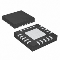
MAX17000ETG+ Maxim Integrated Products, MAX17000ETG+ Datasheet - Page 4

MAX17000ETG+
Manufacturer Part Number
MAX17000ETG+
Description
IC PWM CTLR DDR/DDR2/DDR3 24TQFN
Manufacturer
Maxim Integrated Products
Series
Quick-PWM™r
Type
DDR2/DDR3 Memory Power-Management Solutionr
Datasheet
1.MAX17000ETG.pdf
(32 pages)
Specifications of MAX17000ETG+
Applications
Memory, DDR2/DDR3 Regulator
Current - Supply
2mA
Voltage - Supply
4.5 V ~ 5.5 V
Operating Temperature
-40°C ~ 85°C
Mounting Type
Surface Mount
Package / Case
24-TQFN Exposed Pad
Output Voltage Range
1 V to 2.7 V
Input Voltage Range
3 V to 26 V
Input Current
2 mA
Power Dissipation
2222 mW
Operating Temperature Range
- 40 C to + 85 C
Mounting Style
SMD/SMT
Lead Free Status / RoHS Status
Lead free / RoHS Compliant
Complete DDR2 and DDR3 Memory
Power-Management Solution
ELECTRICAL CHARACTERISTICS (continued)
(V
Typical values are at T
4
REFERENCE BUFFER (VTTR)
VTTR Output Accuracy (Adj)
VTTR Output Accuracy (Preset)
VTTR Maximum
Recommended Current
FAULT DETECTION (SMPS)
SMPS OVP and PGOOD1
Upper Trip Threshold
SMPS OVP and PGOOD1
Upper Trip Threshold
Fault-Propagation Delay
SMPS Output Undervoltage
Fault-Propagation Delay
SMPS PGOOD1 Lower Trip
Threshold
PGOOD1 Lower Trip Threshold
Propagation Delay
PGOOD1 Output Low Voltage
PGOOD1 Leakage Current
TON POR Threshold
FAULT DETECTION (VTT)
PGOOD2 Upper Trip Threshold
PGOOD2 Lower Trip Threshold
PGOOD2 Propagation Delay
PGOOD2 Fault Latch Delay
PGOOD2 Output Low Voltage
PGOOD2 Leakage Current
FAULT DETECTION
Thermal-Shutdown Threshold
V
Threshold
CSL Discharge MOSFET
IN
CC
_______________________________________________________________________________________
= 12V, V
Undervoltage Lockout
PARAMETER
CC
= V
DD
A
= V
= +25°C.) (Note 1)
SHDN
= V
REFIN
V
SYMBOL
t
I
t
I
V
UVLO(VCC)
PGOOD1
PGOOD1
PGOOD2
PGOOD2
T
POR(IN)
t
t
SHDN
OVP
UVP
= 5V, V
REFIN to VTTR
V
Source/sink
FB forced 25mV above trip threshold
Measured at FB, hysteresis = 25mV
FB forced 50mV below PGOOD1 trip
threshold
I
FB = 1V (PGOOD1 high impedance),
PGOOD1 forced to 5V, T
Rising edge, PWM disabled below this level;
hysteresis = 200mV
Hysteresis = 25mV
Hysteresis = 25mV
VTTS forced 50mV beyond PGOOD2
trip threshold
VTTS forced 50mV beyond PGOOD2
trip threshold
I
VTTS = V
PGOOD2 forced to 5V, T
Hysteresis = 15°C
Rising edge, IC disabled below this level
hysteresis = 200mV
OVP = V
CSL
SINK
SINK
CSL
/2 to VTTR
= 1.8V, STDBY = SKIP = AGND, T
= 3mA
= 3mA
CC
REFIN
CONDITIONS
(PGOOD2 high impedance),
I
I
I
I
VTT
VTT
VTT
VTT
A
A
= +25°C
= +25°C
= ±1mA
= ±3mA
= ±1mA
= ±3mA
A
= 0°C to +85°C, unless otherwise noted.
MIN
-10
-20
-10
-20
-12
-13
3.8
12
8
TYP
200
160
-15
3.0
-10
4.1
15
10
10
10
10
16
5
5
MAX
+10
+20
+10
+20
-18
0.4
0.4
4.4
18
13
-8
1
1
UNITS
mA
mV
ms
µA
µA
µs
µs
µs
µs
°C
%
%
%
%
V
V
V
V


