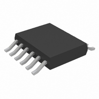
LTC3127EMSE#TRPBF Linear Technology, LTC3127EMSE#TRPBF Datasheet - Page 3

LTC3127EMSE#TRPBF
Manufacturer Part Number
LTC3127EMSE#TRPBF
Description
IC DCDC CONV BUCK BOOST 12MSOP
Manufacturer
Linear Technology
Datasheet
1.LTC3127EDDPBF.pdf
(20 pages)
Specifications of LTC3127EMSE#TRPBF
Applications
Energy Harvesting
Current - Supply
400µA
Voltage - Supply
1.8 V ~ 5.5 V
Operating Temperature
-40°C ~ 85°C
Mounting Type
Surface Mount
Package / Case
12-MSOP Exposed Pad
Lead Free Status / RoHS Status
Lead free / RoHS Compliant
Available stocks
Company
Part Number
Manufacturer
Quantity
Price
elecTrical characTerisTics
temperature range, otherwise specifications are at T
PARAMETER
Input Operating Range
Output Voltage Adjust
Feedback Voltage
Feedback Input Current
Quiescent Current—Burst Mode Operation
Quiescent Current—Shutdown
Quiescent Current—Active
Input Current Limit
Peak Current Limit
Reverse-Current Limit
P-Channel MOSFET Leakage
N-Channel MOSFET On-Resistance
P-Channel MOSFET On-Resistance
Maximum Duty Cycle
Minimum Duty Cycle
Frequency Accuracy
SHDN Input High Voltage
SHDN Input Low Voltage
SHDN Input Current
MODE Input High Voltage
MODE Input Low Voltage
MODE Input Current
Note 1: Stresses beyond those listed under Absolute Maximum Ratings
may cause permanent damage to the device. Exposure to any Absolute
Maximum Rating condition for extended periods may affect device
reliability and lifetime.
Note 2: The LTC3127 is guaranteed to meet performance specifications
from 0°C to 85°C. Specifications over the –40°C to 85°C operating
junction temperature range are assured by design, characterization and
correlation with statistical process controls. Note that the maximum
ambient temperature is determined by specific operating conditions in
conjunction with board layout, the rated package thermal resistance and
other environmental factors.
CONDITIONS
V
V
V
V
R
0°C to 85°C (Note 3)
–40°C to 85°C (Note 3)
Switches A and D
Switch B
Switch C
Switch A
Switch D
Boost( % Switch C On)
Buck (% Switch A On)
V
V
FB
FB
SHDN
FB
SHDN
MODE
PROG
= 1.25V
> 1.225, V
> 1.225V, V
= 0V, Including SW Leakage
= 5.5V
= 32.4k (Note 3)
= 5.5V
J
= 25°C. V
MODE
MODE
The
= V
= 0V (Note 4)
l
IN
IN
denotes the specifications which apply over the full operating
= 3.6V, V
(Note 4)
Note 3: Specification is guaranteed when the inductor current is in
continuous conduction.
Note 4: Current measurements are made when the output is not
switching.
Note 5: This IC includes overtemperature protection that is intended
to protect the device during momentary overload conditions. Junction
temperature will exceed 125°C when overtemperature protection is active.
Continuous operation above the specified maximum operating junction
temperature may result in device degradation or failure.
Note 6: Failure to solder the exposed backside of the package to the PC
board ground plane will result in a thermal resistance much higher than
40°C/W.
OUT
= 3.3V, unless otherwise noted.
l
l
l
l
l
l
l
l
l
l
l
l
l
l
1.165
0.15
MIN
480
465
430
100
1.8
1.8
1.2
1.2
80
2
1
1.195
1.35
0.01
0.01
TYP
400
500
500
500
140
170
160
190
0.1
2.5
0.3
0.1
35
90
1
LTC3127
1.225
MAX
5.25
0.45
520
540
540
5.5
1.7
0.3
0.3
50
4
4
0
1
1
UNITS
MHz
3127f
mΩ
mΩ
mΩ
mΩ
mA
mA
mA
nA
µA
µA
µA
µA
µA
µA
%
%
%
V
V
V
A
A
V
V
V
V


