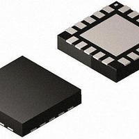
MAX16922ATPA/V+ Maxim Integrated Products, MAX16922ATPA/V+ Datasheet - Page 2

MAX16922ATPA/V+
Manufacturer Part Number
MAX16922ATPA/V+
Description
IC DCDC CONV STPDN DL LDO 20WQFN
Manufacturer
Maxim Integrated Products
Datasheet
1.MAX16922ATPAVT.pdf
(17 pages)
Specifications of MAX16922ATPA/V+
Applications
General Purpose
Current - Supply
5µA
Operating Temperature
-40°C ~ 125°C
Mounting Type
Surface Mount
Package / Case
20-WQFN Exposed Pad, 20-DQFN
Output Voltage
1 V, 2.7 V, 3.3 V, 5 V
Output Current
450 mA, 600 mA, 1.2 A
Switching Frequency
2.2 MHz
Input / Supply Voltage (max)
28 V
Input / Supply Voltage (min)
3.7 V
Maximum Operating Temperature
+ 125 C
Mounting Style
SMD/SMT
Duty Cycle (max)
100 %
Load Regulation
+/- 0.2 %
Minimum Operating Temperature
- 40 C
Number Of Outputs
4
Operating Temperature Range
- 40 C to + 125 C
Supply Current
14 uA
Lead Free Status / RoHS Status
Lead free / RoHS Compliant
Voltage - Supply
-
Lead Free Status / Rohs Status
Lead free / RoHS Compliant
2.2MHz, Dual, Step-Down DC-DC
Converters, Dual LDOs, and RESET
ABSOLUTE MAXIMUM RATINGS
PV1, EN to GND .....................................................-0.3V to +45V
LX1 to GND.................................................-0.5V to (PV1 + 0.3V)
LX2 to GND.................................................-0.5V to (PV2 + 0.3V)
BST to LX1.............................................................-0.3V to +6.0V
PV2, PV3, PV4, OUTS1, PWM, RESET to GND_....-0.3V to +6.0V
OUTS2 .......................................................-0.3V to (PV2 + 0.3V)
OUT3 .........................................................-0.3V to (PV3 + 0.3V)
OUT4 .........................................................-0.3V to (PV4 + 0.3V)
LX1 RMS Current .................................................................2.0A
LX2 RMS Current .................................................................1.2A
PGND2 to GND_....................................................-0.3V to +0.3V
LSUP to GND............................................................-0.3V to +6V
OUTS_, OUT_ Output Short-Circuit Duration .............Continuous
Continuous Power Dissipation (T
ELECTRICAL CHARACTERISTICS
(V
T
Note 1: Package thermal resistances were obtained using the method described in JEDEC specification JESD51-7, using a four-layer
Stresses beyond those listed under “Absolute Maximum Ratings” may cause permanent damage to the device. These are stress ratings only, and functional
operation of the device at these or any other conditions beyond those indicated in the operational sections of the specifications is not implied. Exposure to
absolute maximum rating conditions for extended periods may affect device reliability.
2
OUT1—SYNCHRONOUS STEP-DOWN DC-DC CONVERTER
Supply-Voltage Range
PV1 Undervoltage Lockout
BST Refresh Load Enable
BST Refresh Load Hysteresis
LSUP Regulator Voltage
Supply Current
PWM Switching Frequency
Voltage Accuracy
DMOS On-Resistance
Current-Limit Threshold
Soft-Start Ramp Time
Maximum Output Current
LX1 Leakage Current
Maximum Duty Cycle
Minimum Duty Cycle
A
20-Pin TQFN (derate 31.3 mW/°C above +70°C)............. 2500mW
20-Pin TSSOP (derate 26.5 mW/°C above +70°C)........... 2122mW
PV1
= +25°C under normal conditions, unless otherwise noted.) (Note 2)
_______________________________________________________________________________________
= 13.5V, V
board. For detailed information on package thermal considerations, refer to www.maxim-ic.com/thermal-tutorial.
PARAMETER
PV2
= V
PV3
= V
A
OUT1
= +70°C)
SYMBOL
V
V
, V
DC
DC
V
V
V
UVLO,R
I
UVLO,F
V
OUT1
I
BRLE
LSUP
f
OUT1
PV1
SW
PV1
PV4
MAX
MIN
= V
OUT2
(Note 3)
Operation < 500ms
PV1 rising
PV1 falling
PV1 falling (option enabled)
6V ≤ V
EN = low
Internally generated
Duty cycle = 20% to 90%;
I
SKIP mode (Note 4)
V
(V
V
T
f
LOAD
SW
A
PV1
PV1
OUT1
= -40°C to +85°C
= 2.2MHz
; T
= 4V, V
= 12V, LX1 = GND or V
PV1
= 300mA to 1.2A
+ 1.0V) ≤ V
A
= T
≤ 28V
BST
J
CONDITIONS
= -40°C to +125°C, unless otherwise noted. Typical values are at
= 9V, I
PV1
Junction-to-Case Thermal Resistance (
Junction-to-Ambient Thermal Resistance (
ESD
ESD
ESD
ESD
Operating Temperature Range .........................-40°C to +125°C
Junction Temperature ......................................................+150°C
Storage Temperature Range .............................-65°C to +150°C
Lead Temperature (soldering, 10s) .................................+300°C
Soldering Temperature (reflow) .......................................+260°C
20-Pin TQFN................................................................ 2.7°C/W
20-Pin TSSOP................................................................. 2°C/W
20-Pin TQFN................................................................. 32°C/W
20-Pin TSSOP............................................................ 37.7°C/W
≤ 28V
LX1
HB
MM
CDM
CDM
= 0.2A
(all pins) ...................................................................±2kV
(all pins) ................................................................±200V
PV1
(corner pins) .......................................................±750V
(other pins)..........................................................±500V
;
MIN
2.85
4.75
3.7
2.0
1.4
1.2
-3
-2
TYP
6.45
0.65
1.75
300
3.7
3.3
5.0
2.2
2.2
±1
14
94
20
θ
JC
θ
) (Note 1)
JA
) (Note 1)
MAX
5.45
700
4.0
2.4
2.1
+3
+4
28
45
UNITS
MHz
mΩ
ms
µA
µA
%
%
%
V
V
V
V
V
A
A


