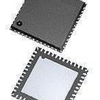
MAX16065ETM+ Maxim Integrated Products, MAX16065ETM+ Datasheet - Page 45

MAX16065ETM+
Manufacturer Part Number
MAX16065ETM+
Description
IC SYSTEM MANAGER 12CH 48-TQFN
Manufacturer
Maxim Integrated Products
Datasheet
1.MAX16065ETM.pdf
(62 pages)
Specifications of MAX16065ETM+
Applications
Power Supply Monitor, Sequencer
Voltage - Supply
2.8 V ~ 14 V
Current - Supply
4.5mA
Operating Temperature
-40°C ~ 85°C
Mounting Type
Surface Mount
Package / Case
48-TQFN Exposed Pad
Number Of Voltages Monitored
12
Undervoltage Threshold
2.7 V
Manual Reset
Resettable
Watchdog
Yes
Battery Backup Switching
No
Power-up Reset Delay (typ)
200 us
Supply Voltage (max)
14 V
Supply Voltage (min)
2.8 V
Supply Current (typ)
10 mA
Maximum Power Dissipation
2222 mW
Mounting Style
SMD/SMT
Maximum Operating Temperature
+ 85 C
Chip Enable Signals
No
Internal Hysteresis
Yes
Minimum Operating Temperature
- 40 C
Power Fail Detection
No
Lead Free Status / RoHS Status
Lead free / RoHS Compliant
Voltage - Input
-
Lead Free Status / Rohs Status
Lead free / RoHS Compliant
The MAX16065/MAX16066 support the SMBus alert
protocol. To enable the SMBus alert output, set r35h[1:0]
according to Table 29, which configures a Fault1, Fault2,
or ANY_FAULT output to act as the SMBus alert. This
output is open-drain and uses the wired-OR configura-
tion with other devices on the SMBus. During a fault,
the MAX16065/MAX16066 assert ALERT low, signaling
the master that an interrupt has occurred. The master
responds by sending the ARA (Alert Response Address)
protocol on the SMBus. This protocol is a read byte with
09h as the slave address. The slave acknowledges the
ARA (09h) address and sends its own SMBus address to
the master. The slave then deasserts ALERT. The master
can then query the slave and determine the cause of the
fault. By checking r1Ch[6], the master can confirm that
the MAX16065/MAX16066 triggered the SMBus alert.
The master must send the ARA before clearing r1Ch[6].
Clear r1Ch[6] by writing a ‘1.’
The MAX16065/MAX16066 feature a JTAG port that
complies with a subset of the IEEE® 1149.1 specifica-
tion. Either the SMBus or the JTAG interface can be used
to access internal memory; however, only one interface
is allowed to run at a time. The MAX16065/MAX16066
do not support IEEE 1149.1 boundary-scan functionality.
The MAX16065/MAX16066 contain extra JTAG instruc-
tions and registers not included in the JTAG specifica-
tion that provide access to internal memory. The extra
instructions include LOAD ADDRESS, WRITE DATA,
READ DATA, REBOOT, SAVE.
IEEE is a registered service mark of the Institute of Electrical
and Electronics Engineers, Inc.
12-Channel/8-Channel, Flash-Configurable System
Table
REGISTER
ADDRESS
35h
29. SMBus Alert Configuration
Managers with Nonvolatile Fault Registers
______________________________________________________________________________________
ADDRESS
FLASH
235h
JTAG Serial Interface
BIT RANGE
[1:0]
SMBALERT
SMBus Alert Configuration:
00 = Disabled
01 = Fault1 is SMBus ALERT
10 = Fault2 is SMBus ALERT
11 = ANY_FAULT is SMBus ALERT
The TAP controller is a finite state machine that responds
to the logic level at TMS on the rising edge of TCK. See
Figure 16 for a diagram of the finite state machine. The
possible states are described in the following:
Test-Logic-Reset: At power-up, the TAP controller
is in the test-logic-reset state. The instruction register
contains the IDCODE instruction. All system logic of the
device operates normally. This state can be reached
from any state by driving TMS high for five clock cycles.
Run-Test/Idle: The run-test/idle state is used between
scan operations or during specific tests. The instruction
register and test data registers remain idle.
Select-DR-Scan: All test data registers retain their previ-
ous state. With TMS low, a rising edge of TCK moves the
controller into the capture-DR state and initiates a scan
sequence. TMS high during a rising edge on TCK moves
the controller to the select-IR-scan state.
Capture-DR: Data can be parallel-loaded into the test
data registers selected by the current instruction. If the
instruction does not call for a parallel load or the selected
test data register does not allow parallel loads, the test
data register remains at its current value. On the rising
edge of TCK, the controller goes to the shift-DR state if
TMS is low or it goes to the exit1-DR state if TMS is high.
Shift-DR: The test data register selected by the current
instruction connects between TDI and TDO and shifts
data one stage toward its serial output on each rising
edge of TCK while TMS is low. On the rising edge of TCK,
the controller goes to the exit1-DR state if TMS is high.
Exit1-DR: While in this state, a rising edge on TCK puts
the controller in the update-DR state. A rising edge on TCK
with TMS low puts the controller in the pause-DR state.
DESCRIPTION
Test Access Port (TAP)
Controller State Machine
45


