SI8252-IQ Silicon Laboratories Inc, SI8252-IQ Datasheet - Page 17
SI8252-IQ
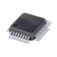
Manufacturer Part Number
SI8252-IQ
Description
IC DIGITAL PWR CONTROLLER 32LQFP
Manufacturer
Silicon Laboratories Inc
Type
SMPS Controllerr
Specifications of SI8252-IQ
Applications
Digital Power Controller
Voltage - Supply
2.25 V ~ 2.75 V
Current - Supply
26mA
Operating Temperature
-40°C ~ 125°C
Mounting Type
Surface Mount
Package / Case
32-LQFP
Product
MOSFET Gate Drivers
Mounting Style
SMD/SMT
For Use With
336-1323 - KIT REFERENCE DESIGN FOR SI825X
Lead Free Status / RoHS Status
Contains lead / RoHS non-compliant
Voltage - Input
-
Lead Free Status / Rohs Status
Lead free / RoHS Compliant
Available stocks
Company
Part Number
Manufacturer
Quantity
Price
Company:

Part Number:
SI8252-IQ
Manufacturer:
Silicon Laboratories Inc
Quantity:
10 000
Company:
Part Number:
SI8252-IQR
Manufacturer:
Silicon Laboratories Inc
Quantity:
10 000


control scheme. The first filter stage is a PID filter
providing one pole and two zeros. The second stage is
selectable: a two-pole, low-pass filter (LPF) for the
fastest possible response, or a SINC (multiple zero)
decimation filter for quieter operation. The PID plus the
LPF result in a three-pole, two-zero composite filter,
while the PID plus the SINC results in a single-pole,
multiple-zero composite filter. The SINC filter provides
zeros at intervals equal to f
decimation ratio (i.e. ratio of input to output sampling
rate). DEC is a software-programmable parameter and
can be programmed such that zero placement occurs at
the PWM frequency and its harmonics. This creates
more than 100 dB attenuation at these frequencies
providing lower system noise levels. The end-to-end
response of the filter is defined using only six software
parameters and can be reprogrammed during converter
operation to implement nonlinear control response for
improved transient resolution.
As described in the ADC1 section above, limit cycle
oscillation can be avoided by increasing ADC1 LSB size
to allow the DPWM LSB to fit within a single ADC1
output code (i.e. zero-error bin). However in some
applications, it may not be desirable to lower ADC1
sensitivity. For such applications, limit cycle oscillation
can be avoided by dithering the DPWM output. The
DSP
broadband noise generator - mixing this noise into the
filter output randomly moves the gate control output(s)
over a range of 1 LSB, such that the time-averaged
resolution of the DPWM is increased.
The filter response is programmed using S-domain
design tools included in the Si8250DK development kit,
greatly minimizing software writing tasks.
3.2.4. Pulse-by-pulse Current Limiter/OCP
High-speed comparator with 4-bit DAC threshold
generator
blanking delay generator. The comparator output
causes the DPWM to terminate the on-going portions of
the active outputs when the peak current signal applied
to the IPK input exceeds the threshold setting.
Hardware performs an OCP supply shutdown when the
number of consecutive current limit events equals a
programmed maximum.
3.2.5. DPWM
Output generator may be programmed for pulse width
(PWM) or phase-shift modulation using design tools
contained in the Si8250DK design kit. The DPWM may
be modulated by the front-end of the Control Processor
(ADC1 and DSP Filter Engine); or by the CPU. The
DPWM has individually programmable stop states for
supply off (disable) and OCP. Software bypass mode
allows the CPU to force selected outputs high or low
Filter
and
Engine
2-bit
contains
programmable
S
/(2*DEC) where DEC is the
a
pseudo-random,
leading-edge
Rev. 1.0
while the remaining outputs continue normal operation.
The DPWM includes an external SYNC input and
ENABLE input, both of which can be connected to the
I/O pins. The Enable is a logic input used to turn the
power supply on and off. It can be configured to be
active high or active low. The SYNC input allows the
start of each switching cycle to be synchronized to an
external clock source, including another Si8250/1/2.
3.3. System Management Processor
3.3.1. ADC0
Self-sequencing, 10-input, 200 Ksps analog-to-digital
converter. This general-purpose ADC acquires other
analog system parameters for supplemental control by
the CPU (e.g. dead time control using average input
current as the control variable). ADC0 also converts the
output of the on-board temperature sensor. Eight of the
ten analog inputs may be connected to the I/O pins for
external interface. The remaining two analog inputs
(V
When placed in Auto Sequencing mode, ADC0
automatically converts, stores and limit-checks each
analog input, and interrupts the CPU when a converted
result is outside of its programmed range. This feature
greatly facilitates protection functions because all
measurement
automated.
3.3.2. Temperature Sensor
This sensor measures the die temperature of the
Si8250/1/2. It can achieve 3 °C accuracy with a single-
point calibration and 1 °C with a two-point calibration.
The temperature output signal is digitized by ADC0.
3.3.3. 8051 CPU
50 MIPS CPU core with 1 kB of SRAM and up to 32 kB
of Flash memory. This processor has its own onboard
oscillator and PLL, reset sources, and real-time in-
system hardware debug interface eliminating the need
for external processor supervisors, timebases, and
"emulators". The CPU has an external interrupt (INT0/)
that can be connected to an external device via the I/O
pins. When interrupted, the CPU suspends execution of
the current task and immediately vectors to an interrupt
service routine specifically designed to handle the
interrupting device.
3.3.4. Digital Peripherals
Peripherals include four 16-bit timers, a three-channel
programmable counter array (PCA, with each channel
useful as a PWM), an SMBus port, a UART (useful as a
serial data port for isolated applications), and two 8-bit
I/O port latches for logic control outputs.
SENSE
Functional Block Descriptions
and Temp Sensor) are internally connected.
and
comparison
Si8250/1/2
operations
are
17
Related parts for SI8252-IQ
Image
Part Number
Description
Manufacturer
Datasheet
Request
R

Part Number:
Description:
MLP 28/A°/3F, 16K, SMPS CONTROLLER
Manufacturer:
Silicon Laboratories Inc
Part Number:
Description:
LQFP 32/A°/NOT RECOMMENDED FOR NEW DESIGNS,3F, 16K, 32 PIN SMPS CONTROLLER
Manufacturer:
Silicon Laboratories Inc

Part Number:
Description:
IC DIGITAL PWR CONTROLLER 32LQFP
Manufacturer:
Silicon Laboratories Inc
Datasheet:
Part Number:
Description:
SMD/C°/SINGLE-ENDED OUTPUT SILICON OSCILLATOR
Manufacturer:
Silicon Laboratories Inc
Part Number:
Description:
Manufacturer:
Silicon Laboratories Inc
Datasheet:
Part Number:
Description:
N/A N/A/SI4010 AES KEYFOB DEMO WITH LCD RX
Manufacturer:
Silicon Laboratories Inc
Datasheet:
Part Number:
Description:
N/A N/A/SI4010 SIMPLIFIED KEY FOB DEMO WITH LED RX
Manufacturer:
Silicon Laboratories Inc
Datasheet:
Part Number:
Description:
N/A/-40 TO 85 OC/EZLINK MODULE; F930/4432 HIGH BAND (REV E/B1)
Manufacturer:
Silicon Laboratories Inc
Part Number:
Description:
EZLink Module; F930/4432 Low Band (rev e/B1)
Manufacturer:
Silicon Laboratories Inc
Part Number:
Description:
I°/4460 10 DBM RADIO TEST CARD 434 MHZ
Manufacturer:
Silicon Laboratories Inc
Part Number:
Description:
I°/4461 14 DBM RADIO TEST CARD 868 MHZ
Manufacturer:
Silicon Laboratories Inc
Part Number:
Description:
I°/4463 20 DBM RFSWITCH RADIO TEST CARD 460 MHZ
Manufacturer:
Silicon Laboratories Inc
Part Number:
Description:
I°/4463 20 DBM RADIO TEST CARD 868 MHZ
Manufacturer:
Silicon Laboratories Inc
Part Number:
Description:
I°/4463 27 DBM RADIO TEST CARD 868 MHZ
Manufacturer:
Silicon Laboratories Inc