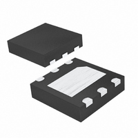
MAX6625RMTT+T Maxim Integrated Products, MAX6625RMTT+T Datasheet - Page 2

MAX6625RMTT+T
Manufacturer Part Number
MAX6625RMTT+T
Description
IC TEMP SENSOR I2C 6-TDFN
Manufacturer
Maxim Integrated Products
Datasheet
1.MAX6625PMTTT.pdf
(17 pages)
Specifications of MAX6625RMTT+T
Function
Temp Monitoring System (Sensor)
Topology
ADC, Comparator, Register Bank
Sensor Type
Internal
Sensing Temperature
-55°C ~ 125°C
Output Type
I²C™/SMBus™
Output Alarm
Yes
Output Fan
Yes
Voltage - Supply
3 V ~ 5.5 V
Operating Temperature
-55°C ~ 125°C
Mounting Type
Surface Mount
Package / Case
6-TDFN Exposed Pad
Full Temp Accuracy
+/- 1 C
Digital Output - Bus Interface
Serial (I2C)
Digital Output - Number Of Bits
9 bit
Maximum Operating Temperature
+ 125 C
Minimum Operating Temperature
- 55 C
Lead Free Status / RoHS Status
Lead free / RoHS Compliant
Other names
MAX6625RMTT+T
MAX6625RMTT+TTR
MAX6625RMTT+TTR
ABSOLUTE MAXIMUM RATINGS
V
OT, SCL, SDA to GND..............................................-0.3V to +6V
ADD to GND .................................................-0.3V to (V
Current into Any Pin............................................................±5mA
OT Sink Current.................................................................. 20mA
9-Bit/12-Bit Temperature Sensors with
I
Note 1: This device is constructed using a unique set of packaging techniques that impose a limit on the thermal profile the device
Stresses beyond those listed under “Absolute Maximum Ratings” may cause permanent damage to the device. These are stress ratings only, and functional
operation of the device at these or any other conditions beyond those indicated in the operational sections of the specifications is not implied. Exposure to
absolute maximum rating conditions for extended periods may affect device reliability.
ELECTRICAL CHARACTERISTICS
(+3V ≤ V
2
S
Power-Supply Voltage
Quiescent Current
ADC Resolution
Temperature Resolution
Accuracy (Notes 2, 3)
Power-Supply Sensitivity
Conversion Time
OT Pullup Resistor
OT Saturation Voltage (Note 4)
OT Delay
T
T
Input High Voltage
Input Low Voltage
Input Hysteresis
I
2
2
HIGH
LOW
to GND ................................................................-0.3V to +6V
C-COMPATIBLE I/O: SCL, SDA, ADD
_______________________________________________________________________________________
C-Compatible Serial Interface in a SOT23
Default Temperature
Default Temperature
can be exposed to during board-level solder attach and rework. This limit permits only the use of the solder profiles recom-
mended in the industry-standard specification, IPC/JEDEC J-STD-020A, paragraph 7.6, Table 3 for IR/VPR and Convection
Reflow. Preheating is required. Hand or wave soldering is not allowed.
S
≤ +5.5V, T
PARAMETER
A =
-55°C to +125°C, unless otherwise noted.)
SYMBOL
T
T
HIGH
V
LOW
V
V
R
V
I
t
C
C
IH
IL
S
P
L
I
I
Shutdown mode
MAX6625
MAX6626
MAX6625
MAX6626
T
0°C = T
0°C = T
V
MAX6625R, MAX6626R only
I
(Programmable through fault queue)
V
V
2
2
OUT
A
S
S
S
C-compatible active
C-compatible inactive
= +25°C, V
= +3V to +5.5V
< +3.6V
> +3.6V
S
= 4mA (Note 4)
+ 0.3V)
A
A
≤ +50°C, V
≤ +70°C, V
S
CONDITIONS
= +3V to +3.6V
Continuous Power Dissipation
Junction Temperature ......................................................+150°C
Storage Temperature Range .............................-60°C to +150°C
ESD Rating (Human Body Model)......................................2000V
Lead Temperature .............................................................Note 1
S
S
= +3.0V to +3.6V
= +3.0V to +3.6V
6-Pin SOT23 (derate 9.1mW/°C above +70°C)............727mW
6-Pin TDFN (derate 23.8mW/°C above +70°C) .........1905mW
1 × t
MIN
3.0
25
2
3
C
0.0625
TYP
250
133
0.5
0.2
12
80
75
1
9
1
6 × t
MAX
±1.5
±2.0
5.5
0.8
0.8
±1
50
1
C
°C/LSB
UNITS
°C/V
Bits
mA
ms
ms
µA
µA
°C
kΩ
°C
°C
V
V
V
V
V


