TC74A1-5.0VAT Microchip Technology, TC74A1-5.0VAT Datasheet - Page 7
TC74A1-5.0VAT
Manufacturer Part Number
TC74A1-5.0VAT
Description
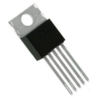
IC DGTL THERM SNSR 5.0V TO220-5
Manufacturer
Microchip Technology
Datasheet
1.TC74A5-3.3VCTTR.pdf
(16 pages)
Specifications of TC74A1-5.0VAT
Package / Case
TO-220-5 (Straight Leads)
Output Type
I²C™/SMBus™
Function
Temp Monitoring System (Sensor)
Topology
ADC (Sigma Delta), Register Bank
Sensor Type
Internal
Sensing Temperature
-40°C ~ 125°C
Output Alarm
No
Output Fan
No
Voltage - Supply
2.7 V ~ 5.5 V
Operating Temperature
-40°C ~ 125°C
Mounting Type
Through Hole
Full Temp Accuracy
3 C
Digital Output - Bus Interface
I2C, SMBus
Digital Output - Number Of Bits
8 bit
Supply Voltage (max)
5.5 V
Supply Voltage (min)
2.7 V
Description/function
Tiny Serial Digital Thermal Sensor
Maximum Operating Temperature
+ 125 C
Minimum Operating Temperature
- 40 C
Supply Current
350 uA
Lead Free Status / RoHS Status
Lead free / RoHS Compliant
Lead Free Status / RoHS Status
Lead free / RoHS Compliant, Lead free / RoHS Compliant
Other names
TC74A15.0VAT
Available stocks
Company
Part Number
Manufacturer
Quantity
Price
Company:

Part Number:
TC74A1-5.0VAT
Manufacturer:
MICROCHIP
Quantity:
12 000


FIGURE 3-1:
3.3
The TC74 continuously monitors the SDA and SCLK
lines for a START condition (a high-to-low transition of
SDA while SCLK is high) and will not respond until this
condition is met.
3.4
Immediately following the START condition, the host
must transmit the address byte to the TC74. The states
of A2, A1 and A0 determine the SMBus/I
the TC74. The 7-bit address transmitted in the serial bit
stream must match for the TC74 to respond with an
Acknowledge (indicating the TC74 is on the bus and
ready to accept data). The 8-bit in the address byte is
a Read/Write bit. This bit is a ‘1’ for a read operation or
‘0’ for a write operation. During the first phase of any
transfer, this bit will be set = 0, indicating that the
command byte is being written.
3.5
Acknowledge (ACK) provides a positive handshake
between the host and the TC74. The host releases
SDA after transmitting 8 bits. The host then generates
a ninth clock cycle to allow the TC74 to pull the SDA
line low. This action acknowledges that the TC74
successfully received the previous 8 bits of data or
address.
2002 Microchip Technology Inc.
Write Byte Format
START Condition (S)
Address Byte
Acknowledge (ACK)
Read Byte Format
Receive Byte Format
S = START Condition
P = STOP Condition
Shaded = Slave Transmission
S
S
Slave Address
S
Address
7 Bits
Address
7 Bits
Slave Address
SMBus/I
Address
7 Bits
WR
RD
2
ACK
C Protocols.
ACK
Command Byte: selects
which register you are
reading from.
Data Byte: reads data from
the register commanded by
the last Read Byte or Write
Byte transmission.
2
WR
Command
C address for
8 Bits
Data
8 Bits
ACK
NACK
ACK
Command Byte: selects
which register you are
writing to.
P
Command
S
8 Bits
Slave Address: repeated
due to change in data-
flow direction.
3.6
After a successful ACK of the address byte, the host
must transmit the data byte to be written, or clock-in the
data to be read (see the appropriate timing diagrams).
ACK will be generated upon a successful write of a
data byte into the TC74.
3.7
Communications must be terminated by a STOP
condition (a low-to-high transition of SDA while SCLK
is high). The STOP condition must be communicated
by the transmitter to the TC74. Refer to Figure 1-1,
“Timing Diagrams”, for serial bus timing.
Address
7 Bits
Data Byte
STOP Condition (P)
ACK
RD
ACK
Data Byte: data goes
into the register set
by the command byte.
8 Bits
Data
Data Byte: reads from
the register set by the
command byte.
8 Bits
Data
ACK
NACK
DS21462C-page 7
TC74
P
P
Related parts for TC74A1-5.0VAT
Image
Part Number
Description
Manufacturer
Datasheet
Request
R

Part Number:
Description:
IC DGTL THERM SNSR 3.3V SOT23A-5
Manufacturer:
Microchip Technology
Datasheet:

Part Number:
Description:
IC DGTL THERM SNSR 3.3V TO220-5
Manufacturer:
Microchip Technology
Datasheet:
Part Number:
Description:
IC DGTL THERM SNSR 3.3V SOT23A-5
Manufacturer:
Microchip Technology
Datasheet:
Part Number:
Description:
IC DGTL THERM SNSR 5.0V SOT23A-5
Manufacturer:
Microchip Technology
Datasheet:

Part Number:
Description:
IC,TEMPERATURE SENSOR,TSOP,5PIN,PLASTIC
Manufacturer:
Microchip Technology
Datasheet:

Part Number:
Description:
Manufacturer:
Microchip Technology Inc.
Datasheet:
Part Number:
Description:
Manufacturer:
Microchip Technology Inc.
Datasheet:
Part Number:
Description:
Manufacturer:
Microchip Technology Inc.
Datasheet:
Part Number:
Description:
Manufacturer:
Microchip Technology Inc.
Datasheet:
Part Number:
Description:
Manufacturer:
Microchip Technology Inc.
Datasheet:
Part Number:
Description:
Manufacturer:
Microchip Technology Inc.
Datasheet: