TC74A7-5.0VAT Microchip Technology, TC74A7-5.0VAT Datasheet - Page 6
TC74A7-5.0VAT
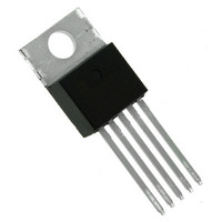
Manufacturer Part Number
TC74A7-5.0VAT
Description
IC DGTL THERM SNSR 5.0V TO220-5
Manufacturer
Microchip Technology
Datasheet
1.TC74A5-3.3VCTTR.pdf
(16 pages)
Specifications of TC74A7-5.0VAT
Package / Case
TO-220-5 (Straight Leads)
Output Type
I²C™/SMBus™
Function
Temp Monitoring System (Sensor)
Topology
ADC (Sigma Delta), Register Bank
Sensor Type
Internal
Sensing Temperature
-40°C ~ 125°C
Output Alarm
No
Output Fan
No
Voltage - Supply
2.7 V ~ 5.5 V
Operating Temperature
-40°C ~ 125°C
Mounting Type
Through Hole
Full Temp Accuracy
3 C
Digital Output - Bus Interface
I2C, SMBus
Digital Output - Number Of Bits
8 bit
Supply Voltage (max)
5.5 V
Supply Voltage (min)
2.7 V
Description/function
Tiny Serial Digital Thermal Sensor
Maximum Operating Temperature
+ 125 C
Minimum Operating Temperature
- 40 C
Supply Current
350 uA
Ic Output Type
Digital
Sensing Accuracy Range
± 2°C
Supply Voltage Range
2.7V To 5.5V
Resolution (bits)
8bit
Sensor Case Style
TO-220
No. Of Pins
5
Accuracy %
0.5°C
Rohs Compliant
Yes
Lead Free Status / RoHS Status
Lead free / RoHS Compliant
Lead Free Status / RoHS Status
Lead free / RoHS Compliant, Lead free / RoHS Compliant
Other names
TC74A75.0VAT
Available stocks
Company
Part Number
Manufacturer
Quantity
Price
Company:

Part Number:
TC74A7-5.0VAT
Manufacturer:
MICROCHIP
Quantity:
12 000


TC74
3.0
3.1
The
information from its onboard solid-state sensor with a
resolution of ±1°C. It stores the data in an internal
register which is then read through the serial port. The
system interface is a slave SMBus/I
which temperature data can be read at any time. Eight
SMBus/I
which allows for a multi-sensor configuration. Also,
there is low power Standby mode when temperature
acquisition is suspended.
3.1.1
The host is allowed, by the TC74, to put it into a low
power (I
mode, the A/D converter is halted and the temperature
data registers are frozen. The SMBus/I
operates normally. Standby mode is enabled by setting
the SHDN bit in the CONFIG register. Table 3-1
summarizes this operation.
TABLE 3-1:
3.1.2
The TC74 is internally programmed to have a default
SMBus/I
addresses are available by custom order (contact
Microchip Technology Inc.
3.2
The Serial Clock input (SCLK) and bidirectional data
port (SDA) form a 2-wire bidirectional serial port for pro-
gramming
conventions used in this bus architecture are listed in
Table 3-2.
DS21462C-page 6
SHDN Bit
0
1
TC74
2
2
DD
DETAILED DESCRIPTION
Functional Description
Serial Port Operation
C addresses are programmable for the TC74,
C address value of 1001 101b. Seven other
STANDBY MODE
SMBUS/I
= 5 µA, typical) Standby mode. In this
and
acquires
STANDBY MODE OPERATION
interrogating
2
C SLAVE ADDRESS
and
Operating Mode
Standby
Normal
converts
the
2
2
C port, through
C port, though,
TC74.
temperature
The
TABLE 3-2:
All transfers take place under the control of a host, usu-
ally a CPU or microcontroller, acting as the Master. This
host provides the clock signal for all transfers. The
TC74 always operates as a Slave. The serial protocol
is illustrated in Figure 3-1. All data transfers have two
phases and all bytes are transferred MSB first.
Accesses are initiated by a START condition, followed
by a device address byte and one or more data bytes.
The device address byte includes a Read/Write selec-
tion bit. Each access must be terminated by a STOP
condition. A convention called “Acknowledge” (ACK)
confirms receipt of each byte. Note that SDA can
change only during periods when SCLK is low (SDA
changes while SCLK is high are reserved for START
and STOP conditions).
Transmitter The device sending data to the bus.
Receiver
Master
Slave
START
STOP
ACK
Busy
NOT Busy
Data Valid
Term
The device receiving data from the bus.
The device which controls the bus initi-
ating transfers (START), generating the
clock and terminating transfers
(STOP).
The device addressed by the master.
A unique condition signaling the begin-
ning of a transfer indicated by SDA
falling (high-low) while SCLK is high.
A unique condition signaling the end of
a transfer indicated by SDA rising (low-
high) while SCLK is high.
A Receiver acknowledges the receipt
of each byte with this unique condition.
The Receiver drives SDA low during
SCLK high of the ACK clock-pulse. The
Master provides the clock pulse for the
ACK cycle.
Communication is not possible
because the bus is in use.
When the bus is idle, both SDA and
SCLK will remain high.
The state of SDA must remain stable
during the high period of SCLK in order
for a data bit to be considered valid.
SDA only changes state while SCLK is
low during normal data transfers (see
START and STOP conditions).
SERIAL BUS CONVENTIONS
2002 Microchip Technology Inc.
Explanation
Related parts for TC74A7-5.0VAT
Image
Part Number
Description
Manufacturer
Datasheet
Request
R

Part Number:
Description:
IC DGTL THERM SNSR 3.3V TO220-5
Manufacturer:
Microchip Technology
Datasheet:

Part Number:
Description:
IC DGTL THERM SNSR 3.3V SOT23A-5
Manufacturer:
Microchip Technology
Datasheet:
Part Number:
Description:
IC DGTL THERM SNSR 3.3V SOT23A-5
Manufacturer:
Microchip Technology
Datasheet:
Part Number:
Description:
IC DGTL THERM SNSR 5.0V SOT23A-5
Manufacturer:
Microchip Technology
Datasheet:

Part Number:
Description:
IC,TEMPERATURE SENSOR,TSOP,5PIN,PLASTIC
Manufacturer:
Microchip Technology
Datasheet:

Part Number:
Description:
Manufacturer:
Microchip Technology Inc.
Datasheet:
Part Number:
Description:
Manufacturer:
Microchip Technology Inc.
Datasheet:
Part Number:
Description:
Manufacturer:
Microchip Technology Inc.
Datasheet:
Part Number:
Description:
Manufacturer:
Microchip Technology Inc.
Datasheet:
Part Number:
Description:
Manufacturer:
Microchip Technology Inc.
Datasheet:
Part Number:
Description:
Manufacturer:
Microchip Technology Inc.
Datasheet: