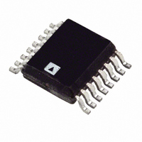
ADT7317ARQ-REEL Analog Devices Inc, ADT7317ARQ-REEL Datasheet - Page 21

ADT7317ARQ-REEL
Manufacturer Part Number
ADT7317ARQ-REEL
Description
IC SENSOR TEMP 10BIT DAC 16QSOP
Manufacturer
Analog Devices Inc
Datasheet
1.ADT7316ARQ.pdf
(44 pages)
Specifications of ADT7317ARQ-REEL
Rohs Status
RoHS non-compliant
Function
Temp Monitoring System (Sensor)
Topology
ADC, Comparator, Multiplexer, Register Bank
Sensor Type
External & Internal
Sensing Temperature
-40°C ~ 120°C, External Sensor
Output Type
I²C™, MICROWIRE™, QSPI™, SMBus™, SPI™
Output Alarm
No
Output Fan
No
Voltage - Supply
2.7 V ~ 5.5 V
Operating Temperature
-40°C ~ 120°C
Mounting Type
Surface Mount
Package / Case
16-QSOP
The buffered/unbuffered option is controlled by the DAC
Configuration register (Address 0x1B; see the Registers
section). The LDAC Configuration register controls the
selection between internal and external voltage references.
The default setting is for external reference to be selected.
OUTPUT AMPLIFIER
The output buffer amplifier is capable of generating output
voltages to within 1 mV of either rail. Its actual range depends
on the value of V
If a gain of 1 is selected (Bit 0 to Bit 3 = 0, DAC Configuration
register, Address 0x1B), the output range is 0.001 V to V
If a gain of 2 is selected (Bit 0 to Bit 3 = 1, DAC Configuration
register, Address 0x1B), the output range is 0.001 V to 2 V
Because of clamping, however, the maximum output is limited
to V
The output amplifier is capable of driving a load of 4.7 kΩ to
V
Figure 6). The source and sink capabilities of the output
amplifier can be seen in Figure 20.
The slew rate is 0.7 V/μs with a half-scale settling time to
±0.5 LSB (at 8 bits) of 6 μs.
THERMAL VOLTAGE OUTPUT
The ADT7316/ADT7317/ADT7318 are capable of outputting
voltages that are proportional to temperature. The DAC A
output can be configured to represent the temperature of the
internal sensor while DAC B output can be configured to
represent the external temperature sensor. Bit C5 and Bit C6
of the Control Configuration 3 register select the temperature
DD
DD
or 4.7 kΩ to GND in parallel with 200 pF to GND (see
– 0.001 V.
2.25V INTERNAL
Figure 42. DAC Reference Buffer Circuit
REF
V
REF
, gain, and offset error.
OPTIONAL CAPACITOR, UP TO
3nF MAX. CAN BE ADDED TO
IMPROVE HIGH FREQUENCY
NOISE REJECTION IN NOISY
ENVIRONMENTS
STRING
STRING
DAC A
DAC B
TRANSISTOR
SENSING
REMOTE
(2N3906)
V
REF
Figure 41. Signal Conditioning for External Diode Temperature Sensors
-AB
D+
C1
D–
LOW-PASS
f
C
REF
FILTER
= 65kHz
REF
.
Rev. B | Page 21 of 44
.
I
DIODE
BIAS
N × I
proportional to output voltage. Each time a temperature
measurement is taken, the DAC output is updated. The out-
put resolution for the ADT7318 is 8 bits with the 1°C change
corresponding to the 1 LSB change. The output resolution for
the ADT7316 and ADT7317 is capable of 10 bits with a 0.25°C
change corresponding to the 1 LSB change.
The default output resolution for the ADT7316 and ADT7317
is 8 bits. To increase this to 10 bits, set C1 = 1 of the Control
Configuration 3 register (Address 0x1A). The default output
range is 0 V to V
2 V
by setting D4 = 1 in the LDAC Configuration register (Address
0x1C). Increasing the output voltage span to 2 V
by setting D0 = 1 for DAC A (internal temperature sensor), and
D1 = 1 for DAC B (external temperature sensor) in the DAC
Configuration register (Address 0x1B).
The output voltage is capable of tracking a maximum tem-
perature range of −128°C to +127°C, but the default setting is
−40°C to +127°C. If the output voltage range is 0 V to V
(V
−40°C, and 1.48 V representing +127°C. This gives an upper
dead band between 1.48 V and V
The internal and external analog temperature offset registers
can be used to vary this upper dead band, and consequently,
the temperature that 0 V corresponds to. Table 6 and Table 7
give examples of how this is done using a DAC output voltage
span of V
value, in twos complement format, at which 0 V is to start. For
example, if using the DAC A output with 0 V to start at −40°C,
program 0xD8 into the internal analog temperature offset regis-
ter (Address 0x21). This is an 8-bit register, and thus, only has a
temperature offset resolution of 1°C for all device models. Use
the following formulas to determine the value to program into
the offset registers.
I
BIAS
REF
REF
-AB = 2.25 V), then this corresponds to 0 V representing
-AB. The user can select the internal V
V
REF
DD
and 2 V
REF
-AB, and this can be increased to 0 V to
ADT7316/ADT7317/ADT7318
REF
, respectively. Write in the temperature
TO ADC
V
V
OUT+
OUT–
REF
-AB.
REF
(V
REF
REF
can be done
= 2.28 V)
REF
-AB


