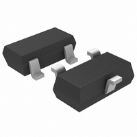
LT1460KCS3-5#TRMPBF Linear Technology, LT1460KCS3-5#TRMPBF Datasheet - Page 17

LT1460KCS3-5#TRMPBF
Manufacturer Part Number
LT1460KCS3-5#TRMPBF
Description
IC REF PREC MICROPWR 5V SOT23
Manufacturer
Linear Technology
Datasheet
1.LT1460EIS8-5.pdf
(26 pages)
Specifications of LT1460KCS3-5#TRMPBF
Reference Type
Series
Voltage - Output
5V
Tolerance
±0.5%
Temperature Coefficient
50ppm/°C
Voltage - Input
5.9 ~ 20 V
Number Of Channels
1
Current - Quiescent
200µA
Current - Output
40mA
Operating Temperature
0°C ~ 70°C
Mounting Type
Surface Mount
Package / Case
SOT-23-3, TO-236-3, Micro3™, SSD3, SST3
Lead Free Status / RoHS Status
Lead free / RoHS Compliant
Current - Cathode
-
Other names
LT1460KCS3-5#PBF
LT1460KCS3-5#PBF
LT1460KCS3-5#PBF
Available stocks
Company
Part Number
Manufacturer
Quantity
Price
applications inForMation
The LT1460S3 family of references are designed to be
stable with a large range of capacitive loads. With no
capacitive load, these references are ideal for fast settling
or applications where PC board space is a premium. The
test circuit shown in Figure 12 is used to measure the
response time and stability of various load currents and
load capacitors. This circuit is set for the 2.5V option. For
other voltage options, the input voltage must be scaled
up and the output voltage generator offset voltage must
be adjusted. The 1V step from 2.5V to 1.5V produces a
current step of 10mA or 1mA for R
Figure 13 shows the response of the reference to these
V
IN
= 2.5V
0.1µF
V
V
V
C
GEN
OUT
OUT
IN
Figure 12. Response Time Test Circuit
LT1460S3-2.5
Figure 13. C
1µs/DIV
V
L
OUT
= 0µF
L
C
L
= 100Ω or R
R
L
1460 F13
V
GEN
2.5V
1.5V
1mA
10mA
L
1460 F12
= 1k.
2.5V
1.5V
1mA and 10mA load steps with no load capacitance, and
Figure 14 shows a 1mA and 10mA load step with a 0.1µF
output capacitor. Figure 15 shows the response to a 1mA
load step with C
The frequency compensation of the LT1460S3 version is
slightly different than that of the other packages. Additional
care must be taken when choosing load capacitance in an
application circuit.
Table 1 gives the maximum output capacitance for vari-
ous load currents and output voltages of the LT1460S3 to
avoid instability. Load capacitors with low ESR (effective
series resistance) cause more ringing than capacitors
with higher ESR such as polarized aluminum or tantalum
capacitors.
V
V
V
V
V
V
GEN
OUT
OUT
GEN
OUT
OUT
L
= 1µF and 4.7µF .
Figure 15. I
Figure 14. C
100µs/DIV
100µs/DIV
OUT
L
= 0.1µF
= 1mA
1460 F14
1460 F15
LT1460
2.5V
1.5V
1mA
10mA
2.5V
1.5V
1µA
4.7µA
1460fc


