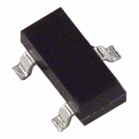
AD1580ART-REEL Analog Devices Inc, AD1580ART-REEL Datasheet - Page 8

AD1580ART-REEL
Manufacturer Part Number
AD1580ART-REEL
Description
IC V-REF 1.225V SOT-23 T/R
Manufacturer
Analog Devices Inc
Datasheet
1.AD1580BRTZ-REEL7.pdf
(12 pages)
Specifications of AD1580ART-REEL
Rohs Status
RoHS non-compliant
Reference Type
Shunt
Voltage - Output
1.225V
Tolerance
±0.1%
Temperature Coefficient
100ppm/°C
Number Of Channels
1
Current - Cathode
50µA
Current - Output
10mA
Operating Temperature
-40°C ~ 85°C
Mounting Type
Surface Mount
Package / Case
SOT-23-3, TO-236-3, Micro3™, SSD3, SST3
Voltage - Input
-
Current - Quiescent
-
Available stocks
Company
Part Number
Manufacturer
Quantity
Price
Part Number:
AD1580ART-REEL
Manufacturer:
ADI/亚德诺
Quantity:
20 000
Company:
Part Number:
AD1580ART-REEL7
Manufacturer:
AD
Quantity:
5 510
Company:
Part Number:
AD1580ART-REEL7
Manufacturer:
HIT
Quantity:
5 510
Part Number:
AD1580ART-REEL7
Manufacturer:
ADI/亚德诺
Quantity:
20 000
AD1580
NOISE PERFORMANCE AND REDUCTION
The noise generated by the AD1580 is typically less than
5 μV p-p over the 0.1 Hz to 10 Hz band. Figure 17 shows the
0.1 Hz to 10 Hz noise of a typical AD1580. Noise in a 10 Hz to
10 kHz bandwidth is approximately 20 μV rms (see Figure 18a).
If further noise reduction is desired, a 1-pole low-pass filter can
be added between the output pin and ground. A time constant
of 0.2 ms has a −3 dB point at about 800 Hz and reduces the
high frequency noise to about 6.5 μV rms (see Figure 18b).
A time constant of 960 ms has a −3 dB point at 165 Hz and
reduces the high frequency noise to about 2.9 μV rms (see
Figure 18c).
TURN-ON TIME
Many low power instrument manufacturers are becoming
increasingly concerned with the turn-on characteristics of
components being used in their systems. Fast turn-on compo-
nents often enable the end user to keep power off when not
needed, and yet those components respond quickly when
the power is turned on for operation. Figure 19 displays the
turn-on characteristic of the AD1580.
20µV/DIV
10µV/DIV
10ms/DIV
1µV/DIV
40µV/DIV
Figure 17. 0.1 Hz to 10 Hz Voltage Noise
Figure 18. Total RMS Noise
6.5µV rms, τ = 0.2ms
2.90µV rms, τ = 960ms
1s/DIV
21µV rms
4.5µV p-p
(a)
(b)
(c)
Rev. D | Page 8 of 12
Upon application of power (cold start), the time required for
the output voltage to reach its final value within a specified
error is the turn-on settling time. Two components normally
associated with this are time for active circuits to settle and time
for thermal gradients on the chip to stabilize. This characteristic
is generated from cold start operation and represents the true
turn-on waveform after power-up. Figure 21 shows both the
coarse and fine turn-on settling characteristics of the device;
the total settling time to within 1.0 mV is about 6 μs, and there
is no long thermal tail when the horizontal scale is expanded to
2 ms/div.
Output turn-on time is modified when an external noise
reduction filter is used. When present, the time constant
of the filter dominates overall settling.
V
0V
V
IN
Figure 20. Turn-On, Settling, and Transient Test Circuit
IN
2.4V
2.4V
250mV/DIV
0V
R
S
= 11.5kΩ
Figure 19. Turn-On Response Time
Figure 21. Turn-On Settling
V
+
–
R
5µs/DIV
OUTPUT ERROR
1mV/DIV, 2µs/DIV
OUTPUT
0.5mV/DIV, 2ms/DIV
V
C
IN
R
L
L
= 200pF
C
L
V
OUT


