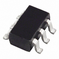
ADR130AUJZ-R2 Analog Devices Inc, ADR130AUJZ-R2 Datasheet

ADR130AUJZ-R2
Specifications of ADR130AUJZ-R2
Related parts for ADR130AUJZ-R2
ADR130AUJZ-R2 Summary of contents
Page 1
FEATURES Initial accuracy A grade: +0.70% (maximum) B grade: +0.35% (maximum) Maximum temperature coefficient A grade: 50 ppm/°C B grade: 25 ppm/° μF LOAD Output current: +4 mA/−2 mA Low operating current: 80 μA ...
Page 2
ADR130 TABLE OF CONTENTS Features .............................................................................................. 1 Applications....................................................................................... 1 Pin Configuration............................................................................. 1 General Description ......................................................................... 1 Revision History ............................................................................... 2 Specifications..................................................................................... 3 Electrical Characteristics............................................................. 3 Absolute Maximum Ratings............................................................ 5 Thermal Resistance ...................................................................... 5 ESD Caution.................................................................................. 5 Typical Performance Characteristics ............................................. ...
Page 3
SPECIFICATIONS ELECTRICAL CHARACTERISTICS T = 25° 2 unless otherwise noted. SET (Pin 5) tied Table 1. Parameter OUTPUT VOLTAGE A Grade B Grade INITIAL ACCURACY ERROR A Grade B Grade ...
Page 4
ADR130 T = 25° 2 unless otherwise noted. SET (Pin 5) tied to GND (Pin 2 Table 2. Parameter OUTPUT VOLTAGE A Grade B Grade INITIAL ACCURACY ERROR A Grade B Grade ...
Page 5
ABSOLUTE MAXIMUM RATINGS Table 3. Parameter V to GND IN Internal Power Dissipation Storage Temperature Range Specified Temperature Range Lead Temperature, Soldering Vapor Phase (60 sec) Infrared (15 sec) Stresses above those listed under Absolute Maximum Ratings may cause permanent ...
Page 6
ADR130 TYPICAL PERFORMANCE CHARACTERISTICS 0.5020 0.5015 0.5010 0.5005 0.5000 0.4995 0.4990 0.4985 0.4980 –40 –25 – TEMPERATURE (°C) Figure 2. V vs. Temperature, V OUT ...
Page 7
ADR130 160 140 +125°C 120 100 INPUT VOLTAGE (V) Figure 8. Supply Current vs. Input Voltage ...
Page 8
ADR130 0.05 0.04 0.03 0.02 0.01 0 –40 –25 – TEMPERATURE (°C) Figure 14. Load Regulation (Source) vs. Temperature, V 1.0 0.9 0.8 0.7 0.6 0.5 0.4 0.3 0.2 0.1 0 –40 –25 – ...
Page 9
0.1µF IN OUT CH1 PEAK-TO-PEAK 172µV TIME (1s/DIV) Figure 20 kHz Noise 0.5 V OUT 0.1µF IN OUT V = 1V/DIV IN V 200mV/DIV OUT TIME ...
Page 10
ADR130 0.1µF IN OUT V = 1V/DIV 20mV/DIV OUT TIME (100µs/DIV) Figure 26. Line Transient Response 0.5V/DIV LOAD 0.1µF IN OUT R = 125Ω LOAD I ...
Page 11
TERMINOLOGY Temperature Coefficient Temperature coefficient is the change of output voltage with respect to the operating temperature change normalized by the output voltage at 25°C. This parameter is expressed in ppm/°C and is determined − ...
Page 12
ADR130 THEORY OF OPERATION The ADR130 sub-band gap reference is the high performance solution for low supply voltage and low power applications. The uniqueness of this product lies in its architecture. POWER DISSIPATION CONSIDERATIONS The ADR130 is capable of delivering ...
Page 13
APPLICATION NOTES BASIC VOLTAGE REFERENCE CONNECTION The circuits in Figure 32 and Figure 33 illustrate the basic configuration for the ADR130 voltage reference. ADR130 GND SET 2 5 INPUT OUT 0.1µF ...
Page 14
ADR130 NEGATIVE PRECISION REFERENCE WITHOUT PRECISION RESISTORS A negative reference is easily generated by adding an op amp, A1, and is configured as shown in Figure 36. V ground and, therefore, the negative reference can be taken directly from the ...
Page 15
... OUTLINE DIMENSIONS INDICATOR 0.10 MAX ORDERING GUIDE Temperature Coefficient Model (ppm/°C) ADR130AUJZ-REEL7 ADR130AUJZ- ADR130BUJZ-REEL7 25 1 ADR130BUJZ- Pb-free part. 2.90 BSC 2.80 BSC 1.60 BSC PIN 1 0.95 BSC 1.90 * 0.90 BSC 0.87 0.84 * 1.00 MAX 0.20 0.08 0.50 SEATING 0.30 PLANE * COMPLIANT TO JEDEC STANDARDS MO-193-AA WITH THE EXCEPTION OF PACKAGE HEIGHT AND THICKNESS ...
Page 16
ADR130 NOTES ©2006 Analog Devices, Inc. All rights reserved. Trademarks and registered trademarks are the property of their respective owners. D06322-0-10/06(0) Rev Page ...


