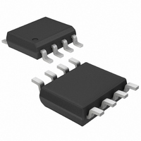
MAX6191BESA Maxim Integrated Products, MAX6191BESA Datasheet - Page 12

MAX6191BESA
Manufacturer Part Number
MAX6191BESA
Description
IC VOLT/REF MICRO PWR LDO 8-SOIC
Manufacturer
Maxim Integrated Products
Datasheet
1.MAX6190CESA.pdf
(14 pages)
Specifications of MAX6191BESA
Reference Type
Series
Voltage - Output
2.048V
Tolerance
±5mV
Temperature Coefficient
10ppm/°C
Voltage - Input
2.5 ~ 12.6 V
Number Of Channels
1
Current - Quiescent
35µA
Current - Output
500µA
Operating Temperature
-40°C ~ 85°C
Mounting Type
Surface Mount
Package / Case
8-SOIC (3.9mm Width)
Product
Voltage References
Topology
Series References
Output Voltage
2.048 V
Average Temperature Coefficient (typ)
4 PPM / C
Series Vref - Input Voltage (max)
13.5 V
Shunt Current (max)
0.5 mA
Maximum Operating Temperature
+ 85 C
Minimum Operating Temperature
- 40 C
Mounting Style
SMD/SMT
Lead Free Status / RoHS Status
Contains lead / RoHS non-compliant
Current - Cathode
-
Lead Free Status / Rohs Status
Lead free / RoHS Compliant
Available stocks
Company
Part Number
Manufacturer
Quantity
Price
Company:
Part Number:
MAX6191BESA+
Manufacturer:
Maxim Integrated Products
Quantity:
135
Precision, Micropower,
Low-Dropout Voltage References
The MAX6190–MAX6195/MAX6198 precision bandgap
references use a proprietary curvature-correction circuit
and laser-trimmed thin-film resistors, resulting in a low
temperature coefficient of <5ppm/°C and initial accura-
cy of better than 0.1%. These devices can sink and
source up to 500µA with <200mV of dropout voltage,
making them attractive for use in low-voltage applica-
tions.
Devices in this family do not require an output capaci-
tance for frequency stability. They are stable for capac-
itive loads from 0 to 2.2nF. However, in applications
where the load or the supply can experience step
changes, an output capacitor will reduce the amount of
overshoot (or undershoot) and assist the circuit’s tran-
sient response. Many applications do not need an
external capacitor, and this family can offer a signifi-
cant advantage in these applications when board
space is critical.
The quiescent supply current of these series-mode ref-
erences is a maximum of 35µA and is virtually indepen-
dent of the supply voltage, with only a 0.8µA/V variation
with supply voltage. Unlike series references, shunt-
mode references operate with a series resistor connect-
ed to the power supply. The quiescent current of a
shunt-mode reference is thus a function of the input
12
1, 3, 5, 7,
PIN
______________________________________________________________________________________
8
2
4
6
NAME
GND
N.C.
OUT
IN
Applications Information
Detailed Description
Output/Load Capacitance
No Connection. Not internally
connected.
Supply Voltage Input
Ground
Reference Voltage Output
Pin Description
FUNCTION
Supply Current
voltage. Additionally, shunt-mode references have to
be biased at the maximum expected load current, even
if the load current is not present all the time. In the
series-mode MAX6190 family, the load current is drawn
from the input voltage only when required, so supply
current is not wasted and efficiency is maximized at all
input voltages. This improved efficiency can help
reduce power dissipation and extend battery life.
When the supply voltage is below the minimum speci-
fied input voltage (as during turn-on), the devices can
draw up to 200µA beyond the nominal supply current.
The input voltage source must be capable of providing
this current to ensure reliable turn-on.
Output voltage hysteresis is the change in the output
voltage at T
cycled over its entire operating temperature range.
Hysteresis is caused by differential package stress
appearing across the bandgap core transistors. The
typical temperature hysteresis value is 75ppm.
These devices typically turn on and settle to within
0.1% of their final value in 30µs to 220µs, depending on
the device. The turn-on time can increase up to 1.5ms
with the device operating at the minimum dropout volt-
age and the maximum load.
Figure 1 shows a typical method for developing a bipo-
lar reference. The circuit uses a MAX681 voltage dou-
bler/inverter charge-pump converter to power an
ICL7652, thus creating a positive as well as a negative
reference voltage.
Positive and Negative Low-Power
A
= +25°C before and after the device is
Output Voltage Hysteresis
Voltage Reference
Turn-On Time


