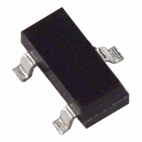
ADR280ART-R2 Analog Devices Inc, ADR280ART-R2 Datasheet - Page 9

ADR280ART-R2
Manufacturer Part Number
ADR280ART-R2
Description
IC REF VOLT HI PSRR 1.2V SOT-23
Manufacturer
Analog Devices Inc
Datasheet
1.ADR280AKSZ-REEL7.pdf
(12 pages)
Specifications of ADR280ART-R2
Rohs Status
RoHS non-compliant
Design Resources
4 mA-to-20 mA Loop-Powered Temperature Monitor Using ADuC7060/1 (CN0145)
Reference Type
Series
Voltage - Output
1.2V
Tolerance
±0.4%
Temperature Coefficient
40ppm/°C
Voltage - Input
2.4 ~ 5.5 V
Number Of Channels
1
Current - Quiescent
16µA
Current - Output
100µA
Operating Temperature
-40°C ~ 85°C
Mounting Type
Surface Mount
Package / Case
SOT-23-3, TO-236-3, Micro3™, SSD3, SST3
Current - Cathode
-
Other names
ADR280ART-R2TR
Boosted Current Source
Adding one more buffer to the previous circuit boosts the
current to the level that is limited only by the buffer U2 current
handling capability (see Figure 18).
Negative Reference
A negative reference can be precisely configured without using
any expensive tight tolerance resistors, as shown in Figure 19.
The voltage difference between V
is at virtual ground, U2 closes the loop by forcing the V− pin to
be the negative reference output.
Boosted Reference with Scalable Output
A precision user defined output with boosted current capability
can be implemented with the circuit shown in Figure 20. In this
circuit, U2 forces V
lating the turn-on of M1; the load current is therefore furnished
by the 5 V supply. For higher output voltage, U2 must be changed
and the supply voltage of M1 and U2 must also be elevated and
separated from the U1 input voltage. In this configuration, a
0.1µF
+5V
230Ω
500Ω
R
C1
SET
RL
5V
Figure 18. Precision Current Source
1.2V
O
Figure 19. Negative Reference
U2
+
–
to be equal to V
I
5mA
L
5V
V+
V–
+
–
+
–
AD8541
U2
U1
U2 = U3 = AD8542, AD822
V+
V–
V+
V
–2.7V
OUT
ADR280
I
L
0.1µF
–
+
= 1.2V/R
U1
C1
OUT
V+
V–
V+
V
OUT
ADR280
U3
V–
and V− is 1.2 V. Since V
REF
5V
SET
× (1 + R2/R1) by regu-
V–
–1.2V
–V
REF
Rev. C | Page 9 of 12
OUT
100 mA load is achievable at a 5 V supply. The higher the
supply voltage, the lower the current handling is because of the
heat generated on the MOSFET. For heavy capacitive loads,
additional buffering is needed at the output to enhance the
transient response.
GSM and 3G Mobile Station Applications
The ADR280 voltage reference is ideal for use with analog
baseband ICs in GSM and 3G mobile station applications.
Figure 21 illustrates the use of the ADR280 with the AD6535
GSM analog baseband. The AD6535 provides all of the data
converters and power management functions needed to
implement a GSM mobile station, including baseband codecs,
audio codecs, voltage regulators, and a battery charger. Besides
low current consumption and a small footprint, the ADR280 is
optimized for excellent PSRR, which is necessary for optimum
AD6535 device performance when the main battery voltage
fluctuates during RF power amplifier activity.
10.8kΩ ± 0.1%
V
10kΩ ± 0.1%
O
25Ω
2.5V/100mA
RL
BASEBAND
DIGITAL
R2
R1
Figure 21. GSM Mobile Station Application
1pF
*M1 = FDB301N, 2N7000, 2N7002, OR EQUIVALENT.
C2
Figure 20. 2.5 V Boosted Reference
VOLTAGE REFERENCE
ANALOG BASEBAND
BASEBAND CODEC
AUDIO CODEC
MANAGEMENT
M1*
U2
ADR280
AD6535
POWER
5V
AD8541
V+
V–
+
–
V
1.2V
REF
C1
0.1µF
U1
V+
V
OUT
ADR280
RADIO
V–
ADR280


