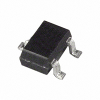
ADR525BKS-REEL7 Analog Devices Inc, ADR525BKS-REEL7 Datasheet - Page 12

ADR525BKS-REEL7
Manufacturer Part Number
ADR525BKS-REEL7
Description
IC REF VOLT SHUNT 2.5V SC-70-3
Manufacturer
Analog Devices Inc
Datasheet
1.ADR520ARTZ-REEL7.pdf
(16 pages)
Specifications of ADR525BKS-REEL7
Rohs Status
RoHS non-compliant
Reference Type
Shunt
Voltage - Output
2.5V
Tolerance
±0.2%
Temperature Coefficient
40ppm/°C
Number Of Channels
1
Current - Cathode
50µA
Current - Output
15mA
Operating Temperature
-40°C ~ 85°C
Mounting Type
Surface Mount
Package / Case
SC-70-3, SOT-323-3
Voltage - Input
-
Current - Quiescent
-
ADR520/ADR525/ADR530/ADR540/ADR550
Stacking the ADR520/ADR525/ADR530/ADR540/ADR550
for User-Definable Outputs
Multiple ADR520/ADR525/ADR530/ADR540/ADR550 parts
can be stacked to allow the user to obtain a desired higher voltage.
Figure 22 shows three ADR550s configured to give 15 V. The bias
resistor, R
bias current flows through all the shunt references in series.
Figure 23 shows three ADR550s stacked to give −15 V. R
is calculated in the same manner as before. Parts of different
voltages can also be added together. For example, an ADR525
and an ADR550 can be added together to give an output of
+7.5 V or −7.5 V, as desired. Note, however, that the initial
accuracy error is now the sum of the errors of all the stacked
parts, as are the temperature coefficients and output voltage
change vs. input current.
BIAS
Figure 22. +15 V Output with Stacked ADR550s
Figure 23. −15 V Output with Stacked ADR550s
, is chosen using Equation 3; note that the same
GND
R
+V
GND
DD
R
–V
ADR550
ADR550
ADR550
DD
+15V
ADR550
ADR550
ADR550
–15V
BIAS
Rev. E | Page 12 of 16
Adjustable Precision Voltage Source
The ADR520/ADR525/ADR530/ADR540/ADR550, combined
with a precision low input bias op amp, such as the AD8610,
can be used to output a precise adjustable voltage. Figure 24
illustrates the implementation of this application using the
ADR520/ADR525/ADR530/ADR540/ADR550. The output
of the op amp, V
which is completely dependent on the resistors, R1 and R2.
An additional capacitor, C1, in parallel with R2, can be added to
filter out high frequency noise. The value of C1 is dependent on
the value of R2.
V
ADR5xx
OUT
= V
V
REF
R
GND
REF
V
S
OUT
(1 + R2 / R1 )
Figure 24. Adjustable Voltage Source
R1
, is determined by the gain of the circuit,
AD8610
(OPTIONAL)
R2
C1
V
OUT
= V
REF
(1+R2/R1)


