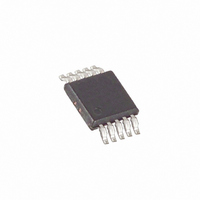
MAX8564EUB+T Maxim Integrated Products, MAX8564EUB+T Datasheet - Page 12

MAX8564EUB+T
Manufacturer Part Number
MAX8564EUB+T
Description
IC CNTRLR N-FET 10-UMAX
Manufacturer
Maxim Integrated Products
Type
Positive Adjustabler
Datasheet
1.MAX8564AEUB.pdf
(15 pages)
Specifications of MAX8564EUB+T
Number Of Outputs
2
Voltage - Output
0.5 ~ 1.8 V, 0.5 ~ 3.3 V
Current - Supply
660µA
Voltage - Input
5V, 12V
Operating Temperature
-40°C ~ 85°C
Package / Case
10-MSOP, Micro10™, 10-uMAX, 10-uSOP
Lead Free Status / RoHS Status
Lead free / RoHS Compliant
For the best transient response in applications with
large step loads (see the Input and Output Capacitor
Selection section for output capacitance requirements),
use the following equations to select the compensation
components:
where C
ESR of C
To use a low-cost ceramic capacitor (see the Input and
Output Capacitor Selection section for load-transient
response characteristics), use the following equations
to select the compensation components:
OUTPUT 1 of Figure 1 is used in this example. Table 1
shows the values required to calculate the compensa-
tion. The values were taken from the appropriate data
sheets and Figure 1.
±1%, Ultra-Low Output Voltage, Dual and Triple
Linear n-FET Controllers
12
Table 1. Parameters Required to
Calculate Compensation
R
PARAMETER CONDITIONS
MOSFET C
MOSFET GFS
V
I
C
R
OUT_MAX
C
OUT1
ESR
OUT1
C
C
______________________________________________________________________________________
C
C
59
OUT
OUT
ISS
g
0 16
g
.
g
is the output capacitance and R
C MAX
R
.
C MAX
C MAX
(
(
C
C
(
V
IDFS = 8.8A
C
OUT
V
Figure 1
Figure 1
Figure 1
Figure 1
DS
V
C
)
x g
)
OUT
)
OUT
15
x V
= 1V
x C
g
V
C MAX
C MAX
OUT
x
(
OUT
(
x g
C
OUT
C
OUT
C
)
C MAX
)
I
(
x g
OUT MAX
C
g
VALUE
I
OUT
C MAX
R
2500
OUT MAX
100
V
1.5
1.5
(
30
18
ESR
C MAX
OUT
_
)
(
_
)
1
)
x R
2
I
OUT
ESR
ESR
Example
UNITS
C
C
_
m
pF
µF
S
V
A
ISS
MAX
MAX
ISS
is the
1
Due to the high-current paths and tight output accuracy
required by most applications, careful PC board layout is
required. An evaluation kit (MAX8563EVKIT) is available
to speed design.
It is important to keep all traces as short as possible to
maximize the high-current trace dimensions to reduce the
effect of undesirable parasitic inductance. The MOSFET
dissipates a fair amount of heat due to the high currents
involved, especially during large input-to-output voltage
differences. To dissipate the heat generated by the
MOSFET, make power traces very wide with a large
amount of copper area. An efficient way to achieve good
power dissipation on a surface-mount package is to lay
out copper areas directly under the MOSFET package on
multiple layers and connect the areas through vias. Use a
ground plane to minimize impedance and inductance. In
addition to the usual high-power considerations, here are
four tips to ensure high output accuracy:
•
•
•
•
C
C
Ensure that the feedback connection to C
short and direct.
Place the feedback resistors next to the FB pin.
Place R
Ensure FB_ and DRV_ traces are away from noisy
sources to ensure tight accuracy.
R R
C
0 16
.
59
g
C
C MAX
and C
(
x
x
1 5
1 5
.
.
2500
)
V x
V x
PC Board Layout Guidelines
C
1
next to the DRV_ pin.
599 4
12 4
F
pF
100
30
100
12 4
.
S x
.
S x
.
F x
F x
S x
0 90
,
.
use
1 5
1 5
8 8
12 4
.
1 5
.
12 4
.
F use
V
.
.
A
A
620
,
.
V
S x
S x
1 5
12 4
.
.
1 5
1
.
A
18
.
12 4
18
S
F
A
2
m
.
m
.
S x
OUT_
1
1
is


