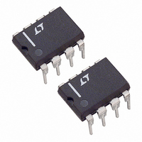
LT1245IN8 Linear Technology, LT1245IN8 Datasheet - Page 8

LT1245IN8
Manufacturer Part Number
LT1245IN8
Description
IC PWM CURRNT MODE HI-SPEED 8DIP
Manufacturer
Linear Technology
Datasheet
1.LT1245IN8.pdf
(16 pages)
Specifications of LT1245IN8
Pwm Type
Current Mode
Number Of Outputs
1
Frequency - Max
500kHz
Duty Cycle
48%
Voltage - Supply
8.2 V ~ 25 V
Buck
Yes
Boost
No
Flyback
No
Inverting
No
Doubler
No
Divider
No
Cuk
No
Isolated
Yes
Operating Temperature
-40°C ~ 100°C
Package / Case
8-DIP (0.300", 7.62mm)
Frequency-max
500kHz
Lead Free Status / RoHS Status
Contains lead / RoHS non-compliant
Available stocks
Company
Part Number
Manufacturer
Quantity
Price
Part Number:
LT1245IN8#PBF
Manufacturer:
LINEAR/凌特
Quantity:
20 000
for various values of R
Performance Characteristics section. Frequency and
deadtime can also be calculated using the following
formulas:
LT1241 Series
A
The above formulas will give values that will be accurate
to approximately 5%, at the oscillator, over the full
operating frequency range. This is due to the fact that the
oscillator trip levels are constant versus frequency and the
discharge current and initial oscillator frequency are
trimmed. Some fine adjustment may be required to achieve
more accurate results. Once the final R
selected the oscillator characteristics will be repeatable
from device to device. Note that there will be some slight
differences between maximum duty cycle at the oscillator
and maximum duty cycle at the output due to the finite rise
and fall times of the output.
The output switching frequency will be equal to the
oscillator frequency for LT1242 and LT1243. The output
switching frequency will be equal to one-half the oscillator
8
Oscillator Rise Time: t
Oscillator Discharge Time:
Oscillator Period: T
Oscillator Frequency:
Maximum Duty Cycle:
LT1241, LT1244, LT1245
LT1242, LT1243
PPLICATI
D
MAX
2
T
t
OSC
r
O
U
D
OSC
MAX
S
T
OSC
2
T
r
f
OSC
= t
= 0.583 • RC
I FOR ATIO
T
and C
U
OSC
r
t
+ t
T
t
d
OSC
d
t
T
r
d
T
OSC
1
appear in the Typical
0 0164
W
T
T
OSC
/C
3 46
T
T
OSC
combination is
R
t
RC
d
11 73
U
frequency for LT1241, LT1244 and LT1245. The oscillator
of LT1241 series devices will run at frequencies up to
1MHz, allowing 500kHz output switching frequencies for
all devices.
Error Amplifier
The LT1241 series of devices contain a fully compensated
error amplifier with a DC gain of 90dB and a unity-gain
frequency of 1MHz. Phase margin at unity-gain is 80 . The
noninverting input is internally committed to a 2.5V refer-
ence point derived from the 5V reference of Pin 8. The
inverting input (Pin 2) and the output (Pin 1) are made
available to the user. The output voltage in a regulator
circuit is normally fed back to the inverting input of the
error amplifier through a resistive divider.
The output of the error amplifier is made available for
external loop compensation. The output current of the
error amplifier is limited to approximately 0.8mA sourcing
and approximately 6mA sinking. In a current mode PWM
the peak switch current is a function of the output voltage
of the error amplifier. In the LT1241 series devices the
output of the error amplifier is offset by two diodes (1.4V
at 25 C), divided by a factor of three, and fed to the
inverting input of the current sense comparator. For error
amplifier output voltages less than 1.4V the duty cycle of
the output stage will be zero. The maximum offset that can
appear at the current sense input is limited by a 1V clamp.
This occurs when the error amplifier output reaches 4.4V
at 25 C.
The output of the error amplifier can be clamped below
4.4V in order to reduce the maximum voltage allowed
across the current sensing resistor to less than 1V. The
supply current will increase by the value of the output
source current when the output voltage of the error
amplifier is clamped.


