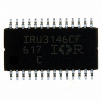
IRU3146CFTR International Rectifier, IRU3146CFTR Datasheet - Page 6

IRU3146CFTR
Manufacturer Part Number
IRU3146CFTR
Description
IC PWM DUAL SYNC 28-TSSOP
Manufacturer
International Rectifier
Specifications of IRU3146CFTR
Pwm Type
Voltage Mode
Number Of Outputs
2
Frequency - Max
345kHz
Duty Cycle
85%
Voltage - Supply
4.5 V ~ 16 V
Buck
Yes
Boost
No
Flyback
No
Inverting
No
Doubler
No
Divider
No
Cuk
No
Isolated
No
Operating Temperature
0°C ~ 70°C
Package / Case
28-TSSOP
Frequency-max
345kHz
Lead Free Status / RoHS Status
Contains lead / RoHS non-compliant
IRU3146
FUNCTIONAL DESCRIPTION
Introduction
The IRU3146 is versatile device for high performance Buck
converters. It is included of two synchronous Buck con-
trollers which can be operated both in two independent
mode or in 2-phase mode.
The timing of the IC is provided through an internal oscil-
lator circuit. These are two out-of-phase oscillators that
can be programmed up to 400KHz per phase.
Supply Voltage
Vcc is the supply voltage for internal controller. The op-
erating range is from 4.5V to 16V. It also is fed to the
internal LDO. When Vcc is below under-voltage thresh-
old, all MOSFET drivers will be turned off.
Internal Regulator
The regulator powers directly from VCC and generates a
regulated voltage (Typ. 6.2V@50mA). The output is pro-
tected for short circuit. This voltage can be used for charge
pump circuitry as describe in Figure12.
Input Supplies UnderVoltage LockOut
The IRU3146 UVLO block monitors three input voltages
(VCC, VCH1 and VCH2) to ensure reliable start up. The
MOSFET driver output turn off when any of the supply
voltages drops below set thresholds. Normal operation
resumes once the supply voltages rise above the set
values.
Independent Mode
In this mode the IRU3146 provides control to two inde-
pendent output power supplies with either common or
different input voltages. The output voltage of each indi-
vidual channel is set and controlled by the output of the
error amplifier, which is the amplified error signal from
the sensed output voltage and the reference voltage. The
error amplifier output voltage is compared to the ramp
signal thus generating fixed frequency pulses of variable
duty-cycle, which are applied to the FET drivers, Fig-
ure18 shows a typical schematic for such application.
2-Phase Mode
This feature allows to connect both outputs together to
increase current handling capability of the converter to
support a common load. The current sharing can be done
either using external resistors or sensing the DCR of
inductors (see Figure 4). In this mode, one control loop
acts as a master and sets the output voltage as a regu-
lar Voltage Mode Buck controller and the other control
loop acts as a slave and monitors the current
6
www.irf.com
information for current sharing. The voltage drops across
the current sense resistors (or DCR of inductors) are
measured and their difference is amplified by the slave
error amplifier and compared with the ramp signal to
generate the PWM pulses to match the output current.
In this mode the SS2 pin should be floating.
In the diagram, L1 and L2 are the output inductors. R
and R
R1 and capacitor C1 are used to sense the average in-
ductor current. The voltage across the capacitors C1
and C2 represent the average current flowing into resis-
tance R
should be equal or at most three times larger than the
time constant L
Figure 5 - 30A Current Sharing using Inductor sensing
PWM Comp2
PWM Comp1
Figure 4 - Loss-less inductive current sensing
L2
R1×C1=(1~3)×
L1
are inherent inductor resistances. The resistor
and R
L2
1
Master E/A
/R
IRU3146
and current sharing.
. The time constant of the RC network
Slave E/A
L1
.
(5A/Div)
R
0.8V
L1
Fb1
FB2
Comp
VP2
L1
---(1)
R1
R2
L1
L2
C1
C2
R
R
L1
L2
Rev. 1.1
6/25/04
V
OUT
L1


