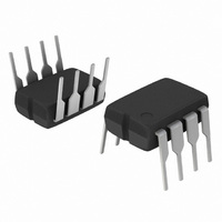
UC3844BNG ON Semiconductor, UC3844BNG Datasheet - Page 2

UC3844BNG
Manufacturer Part Number
UC3844BNG
Description
IC CTLR CURRENT MODE 8-DIP
Manufacturer
ON Semiconductor
Type
Pulse Width Modulator Controllerr
Specifications of UC3844BNG
Pwm Type
Current Mode
Number Of Outputs
1
Frequency - Max
275kHz
Duty Cycle
50%
Voltage - Supply
11.5 V ~ 25 V
Buck
No
Boost
Yes
Flyback
Yes
Inverting
Yes
Doubler
No
Divider
No
Cuk
No
Isolated
Yes
Operating Temperature
0°C ~ 70°C
Package / Case
8-DIP (0.300", 7.62mm)
Frequency-max
275kHz
Number Of Pwm Outputs
1
On/off Pin
No
Adjustable Output
No
Topology
Boost/Flyback
Switching Freq
500KHz
Operating Supply Voltage (max)
30V
Output Current
1000A
Synchronous Pin
No
Rise Time
50ns
Fall Time
50ns
Operating Temperature Classification
Commercial
Mounting
Through Hole
Pin Count
8
Package Type
PDIP
Duty Cycle (max)
48 % (Typ)
Output Voltage
4.9 V to 5.1 V
Mounting Style
Through Hole
Switching Frequency
500 KHz
Operating Supply Voltage
30 V
Maximum Operating Temperature
70 C
Minimum Operating Temperature
0 C
Current, Input Bias
-2 μA
Current, Output
+12 mA (Sink), -1 mA (Source)
Current, Supply
30 mA
Frequency, Oscillator
250 kHz
Power Dissipation
1.25 W
Regulation, Line
2 mV
Regulation, Load
3 mV
Regulator Type
DC-DC
Temperature, Operating, Range
0 to +70 °C
Time, Fall
50 ns
Time, Rise
50 ns
Voltage, Gain
3 V/V
Voltage, Input
-0.3 to +5.5 V
Voltage, Noise
50 μV
Voltage, Output
5 V
Voltage, Output, High
13.5 V
Voltage, Output, Low
1.6 V
Voltage, Supply
36 V
Voltage, Supply, Rejection Ratio
70 dB
Lead Free Status / RoHS Status
Lead free / RoHS Compliant
Other names
UC3844BNGOS
Available stocks
Company
Part Number
Manufacturer
Quantity
Price
Part Number:
UC3844BNG
Manufacturer:
ON/安森美
Quantity:
20 000
Stresses exceeding Maximum Ratings may damage the device. Maximum Ratings are stress ratings only. Functional operation above the
Recommended Operating Conditions is not implied. Extended exposure to stresses above the Recommended Operating Conditions may affect
device reliability.
1. The voltage is clamped by a zener diode (see page 9 Under Voltage Lockout section). Therefore this voltage may be exceeded as long as
2. Maximum package power dissipation limits must be observed.
3. This device series contains ESD protection and exceeds the following tests:
4. This device contains latch-up protection and exceeds 100 mA per JEDEC Standard JESD78
5. Adjust V
6. Low duty cycle pulse techniques are used during test to maintain junction temperature as close to ambient as possible.
MAXIMUM RATINGS
ELECTRICAL CHARACTERISTICS
T
REFERENCE SECTION
OSCILLATOR SECTION
Bias and Driver Voltages (Zero Series Impedance, see also Total Device spec) (Note 1)
Total Power Supply and Zener Current
Output Current, Source or Sink (Note 2)
Output Energy (Capacitive Load per Cycle)
Current Sense and Voltage Feedback Inputs
Error Amp Output Sink Current
Power Dissipation and Thermal Characteristics
D Suffix, Plastic Package, SOIC−14 Case 751A
D1 Suffix, Plastic Package, SOIC−8 Case 751
N Suffix, Plastic Package, Case 626
Operating Junction Temperature
Operating Ambient Temperature
Storage Temperature Range
A
Reference Output Voltage (I
Line Regulation (V
Load Regulation (I
Temperature Stability
Total Output Variation over Line, Load, and Temperature
Output Noise Voltage (f = 10 Hz to 10 kHz, T
Long Term Stability (T
Output Short Circuit Current
Frequency
Frequency Change with Voltage (V
Frequency Change with Temperature (T
Oscillator Voltage Swing (Peak−to−Peak)
the total power supply and zener current is not exceeded.
T
is the operating ambient temperature range that applies [Note 6], unless otherwise noted.)
Maximum Power Dissipation @ T
Thermal Resistance, Junction−to−Air
Maximum Power Dissipation @ T
Thermal Resistance, Junction−to−Air
Maximum Power Dissipation @ T
Thermal Resistance, Junction−to−Air
T
T
T
low
Human Body Model 4000 V per JEDEC Standard JESD22-A114B
Machine Model Method 200 V per JEDEC Standard JESD22-A115-A
A
J
J
= 25°C
= 25°C (R
= T
= 0°C for UC3844B, UC3845B
= − 25°C for UC2844B, UC2845B
= − 40°C for UC3844BV, UC3845BV
low
CC
to T
above the Startup threshold before setting to 15 V.
T
high
= 6.2 k, C
O
CC
= 1.0 mA to 20 mA)
Characteristic
A
= 12 V to 25 V)
= 125°C for 1000 Hours)
T
O
= 1.0 nF)
= 1.0 mA, T
CC
A
A
A
= 25°C
= 25°C
= 25°C
= 12 V to 25 V)
A
Rating
(V
= T
J
= 25°C)
CC
J
low
= 25°C)
= 15 V [Note 5], R
to T
T
high
high
= + 70°C for UC3844B, UC3845B
= + 85°C for UC2844B, UC2845B
= +105°C for UC3844BV, UC3845BV
)
http://onsemi.com
Df
Df
Symbol
Reg
Reg
OSC
V
OSC
f
UC3844B, UC3845B
UC2844B, UC2845B
T
V
V
I
OSC
T
V
OSC
SC
S
ref
ref
2
= 10 k, C
S
n
load
line
/DV
/DT
T
4.95
− 30
Min
= 3.3 nF. For typical values T
225
4.9
49
48
−
−
−
−
−
−
−
−
UC284XB
− 85
Typ
250
5.0
2.0
3.0
0.2
5.0
0.2
1.0
1.6
50
52
−
−
(I
V
Symbol
−180
Max
5.05
CC
275
CC
5.1
1.0
R
R
R
20
25
55
56
T
−
−
−
−
−
V
P
P
P
T
T
I
W
I
qJA
qJA
qJA
stg
O
O
, V
in
A
+ I
D
D
D
J
Z
C
)
4.82
− 30
Min
225
4.9
49
48
−
−
−
−
−
−
−
−
A
UC384XB, XBV
= 25°C, for min/max values
− 0.3 to + 5.5
− 65 to +150
− 25 to + 85
0 to + 70
− 85
Typ
250
5.0
2.0
3.0
0.2
5.0
0.2
0.5
1.6
50
52
Value
+150
−
−
1.25
862
145
702
178
100
1.0
5.0
36
30
10
−180
Max
5.18
275
5.1
1.0
20
25
55
56
−
−
−
−
−
°C/W
°C/W
°C/W
mV/°C
Unit
mW
mW
mA
mA
Unit
°C
°C
°C
kHz
mJ
W
mV
mV
mV
mA
V
A
V
mV
%
%
V
V
V


