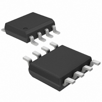
MAX5070BASA+T Maxim Integrated Products, MAX5070BASA+T Datasheet - Page 14

MAX5070BASA+T
Manufacturer Part Number
MAX5070BASA+T
Description
IC CNTRLR PWM CRNT MD 8-SOIC
Manufacturer
Maxim Integrated Products
Datasheet
1.MAX5070BAUA.pdf
(22 pages)
Specifications of MAX5070BASA+T
Pwm Type
Current Mode
Number Of Outputs
1
Frequency - Max
1MHz
Duty Cycle
50%
Voltage - Supply
10.8 V ~ 25 V
Buck
No
Boost
No
Flyback
Yes
Inverting
No
Doubler
No
Divider
Yes
Cuk
No
Isolated
Yes
Operating Temperature
-40°C ~ 125°C
Package / Case
8-SOIC (3.9mm Width)
Frequency-max
1MHz
Duty Cycle (max)
50%
Output Current
2000 mA
Mounting Style
SMD/SMT
Switching Frequency
1000 KHz
Maximum Operating Temperature
+ 125 C
Fall Time
22 ns
Minimum Operating Temperature
- 40 C
Rise Time
15 ns
Synchronous Pin
No
Topology
Flyback, Forward, Push-Pull
Lead Free Status / RoHS Status
Lead free / RoHS Compliant
To calculate the capacitance required, use the following
formula:
where:
I
ply current after startup (see the Typical Operating
Characteristics to find the I
total gate charge for the MOSFET, f
switching frequency, V
teresis (6V), and t
by external circuitry.
Size the resistor R
time period, t
ing equations to calculate the average charging current
(I
Where V
the application (36V for telecom), V
strap UVLO wake-up level (16V), and I
supply current at startup (65µA, max). Choose a higher
value for R
startup times can be tolerated in order to minimize
power loss in R
The above startup method is applicable to circuits where
the tertiary winding has the same phase as the output
windings. Thus, the voltage on the tertiary winding at any
given time is proportional to the output voltage and goes
through the same soft-start period as the output voltage.
The minimum discharge time of C
must be greater than the soft-start time (t
High-Performance, Single-Ended, Current-Mode
PWM Controllers
14
CC
CST
is the MAX5070/MAX5071s’ maximum internal sup-
______________________________________________________________________________________
) and the startup resistor (R
C
INMIN
ST
ST
=
ST
than the one calculated above if longer
R
is the minimum input supply voltage for
⎡
⎢
⎢
⎣
ST
, for the calculated C
I
CC
ST
I
.
CST
SS
ST
≅
+
I
⎛
⎜
⎝
G
I
is the soft-start time, which is set
according to the desired startup
G
=
V
HYST
INMIN
I
−
CST
V
= Q
⎛
⎜
⎝
SUVR
V
IN
V
INMIN
G
is the bootstrap UVLO hys-
HYST
+
t
at a given f
−
ST
I
f
R
START
SW
×
V
ST
ST
SUVR
C
−
2
).
ST
13
ST
SW
ST
V
SUVR
⎞
⎟
⎠
from 16V to 10V
SS
⎞
⎟
⎠
. Use the follow-
START
is the converter
⎤
⎥
⎥
⎦
OSC
( )
).
t
SS
is the boot-
). Q
is the V
G
is the
IN
The minimum turn-on supply voltage for the
MAX5070/MAX5071 is 16V. Once V
reference powers up. There is 6V of hysteresis from the
minimum turn-on voltage to the UVLO threshold. Once
V
with V
device is in UVLO. When in UVLO, the quiescent sup-
ply current into V
and VREF are pulled low.
OUT drives an external n-channel MOSFET and swings
from GND to V
absolute maximum V
OUT is a push-pull output with the on-resistance of the
PMOS typically 3.5Ω and the on-resistance of the NMOS
typically 4.5Ω. The driver can source 2A typically and
sink 1A typically. This allows for the MAX5070/MAX5071
to quickly turn on and off high gate-charge MOSFETs.
Bypass V
to GND, placed close to the MAX5070/MAX5071. The
average current sourced to drive the external MOSFET
depends on the total gate charge (Q
frequency of the converter. The power dissipation in the
MAX5070/MAX5071 is a function of the average output
drive current (I
culate the power dissipation in the device due to I
where I
Typical Operating Characteristics for the operating
supply current at a given frequency.
The MAX5070 includes an internal error amplifier. The
inverting input is at FB and the noninverting input is inter-
nally connected to a 2.5V reference. The internal error
amplifier is useful for nonisolated converter design (see
Figure 6) and isolated design with primary-side regulation
through a bias winding (see Figure 5). In the case of a
nonisolated power supply, the output voltage will be:
where R1 and R2 are from Figure 6.
CC
reaches 16V, the MAX5070/MAX5071 will operate
Error Amplifier (MAX5070A/MAX5070B)
CC
CC
CC
down to 10V. Once V
is the operating supply current. See the
with one or more 0.1µF ceramic capacitors
DRIVE
PD = (I
CC
V
Undervoltage Lockout (UVLO)
OUT
CC
. Ensure that V
I
DRIVE
). Use the following equation to cal-
falls back to 37µA (typ), and OUT
GS
DRIVE
=
⎛
⎜
⎝
rating of the external MOSFET.
1
= Q
+
+ I
R
R
G
2
1
CC
⎞
⎟ ×
⎠
CC
x f
CC
) x V
SW
2 5 .
CC
goes below 10V the
MOSFET Driver
remains below the
V
G
CC
reaches 16V, the
) and operating
DRIVE
:


