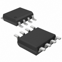
MAX5015ESA+T Maxim Integrated Products, MAX5015ESA+T Datasheet - Page 6

MAX5015ESA+T
Manufacturer Part Number
MAX5015ESA+T
Description
IC CNTRLR PWM CRNT MD 8-SOIC
Manufacturer
Maxim Integrated Products
Datasheet
1.MAX5015ESA.pdf
(14 pages)
Specifications of MAX5015ESA+T
Pwm Type
Current Mode
Number Of Outputs
1
Frequency - Max
275kHz
Duty Cycle
50%
Voltage - Supply
18 V ~ 110 V
Buck
No
Boost
No
Flyback
No
Inverting
No
Doubler
No
Divider
No
Cuk
No
Isolated
Yes
Operating Temperature
-40°C ~ 85°C
Package / Case
8-SOIC (3.9mm Width)
Frequency-max
275kHz
Duty Cycle (max)
50 %
Output Current
1000 mA
Mounting Style
SMD/SMT
Switching Frequency
275 KHz
Maximum Operating Temperature
+ 85 C
Minimum Operating Temperature
- 40 C
Synchronous Pin
No
Topology
Flyback, Forward
Lead Free Status / RoHS Status
Lead free / RoHS Compliant
Use the MAX5014/MAX5015 PWM current-mode con-
trollers to design flyback- or forward-mode power sup-
plies. Current-mode operation simplifies control-loop
design while enhancing loop stability. An internal high-
voltage startup regulator allows the device to connect
directly to the input supply without an external startup
resistor. Current from the internal regulator starts the
controller. Once the tertiary winding voltage is estab-
lished the internal regulator is switched off and bias
current for running the IC is derived from the tertiary
winding. The internal oscillator is set to 275kHz and
trimmed to ±10%. This permits the use of small mag-
netic components to minimize board space. Both the
MAX5014 and MAX5015 can be used in power sup-
plies providing multiple output voltages. A functional
diagram of the IC is shown in Figure 1. Typical applica-
tions circuits for forward and flyback topologies are
shown in Figure 2 and Figure 3, respectively.
The MAX5014/MAX5015 offer current-mode control
operation with added features such as leading-edge
blanking with dual internal path that only blanks the
sensed current signal applied to the input of the PWM
comparator. The current limit comparator monitors the
CS pin at all times and provides cycle-by-cycle current
Current-Mode PWM Controllers with Integrated
Startup Circuit for Isolated Power Supplies
6
_______________________________________________________________________________________
PIN
1
2
3
4
5
6
7
8
SS_SHDN
NAME
OPTO
NDRV
GND
V
V
V+
CS
DD
CC
Detailed Description
High-Voltage Startup Input. Connect directly to an input voltage between 18V to 110V. Connects
internally to a high-voltage linear regulator that generates V
V
and V+ can both be connected to the supply. For supply voltages greater than 36V, V
its power from the tertiary winding of the transformer and accepts voltages from 13V to 36V. Bypass
to GND with a 4.7µF capacitor.
Optocoupler Input. The control voltage range on this input is 2V to 3V.
Soft-Start Timing Capacitor Connection. Ramp time to full current limit is approximately 0.45ms/nF.
This pin is also the reference voltage output. Bypass with a minimum 10nF capacitor to GND. The
device goes into shutdown when V
Current Sense Input. Turns power switch off if V
limiting. CS is also the feedback for the current-mode controller. CS is connected to the PWM
comparator through a leading edge blanking circuit.
Ground
Gate Drive. Drives a high-voltage external N-channel power MOSFET.
Regulated IC Supply. Provides power for the entire IC. V
operation and from V+ during startup. Bypass V
0.1µF ceramic capacitor to GND.
Current-Mode Control
DD
is the Input of the Linear Regulator that Generates V
SS_SHDN
limit without being blanked. The leading-edge blanking
of the CS signal prevents the PWM comparator from
prematurely terminating the on cycle. The CS signal
contains a leading-edge spike that is the result of the
MOSFET gate charge current, capacitive and diode
reverse recovery current of the power circuit. Since this
leading-edge spike is normally lower than the current
limit comparator threshold, current limiting is not
blanked and cycle-by-cycle current limiting is provided
under all conditions.
Use the MAX5014 in discontinuous flyback applications
where wide line voltage and load current variation is
expected. Use the MAX5015 for single transistor for-
ward converters where the maximum duty cycle must
be limited to less than 50%.
Under certain conditions it may be advantageous to
use a forward converter with greater than 50% duty
cycle. For those cases use the MAX5014. The large
duty cycle results in much lower operating primary
RMS currents through the MOSFET switch and in most
cases a smaller output filter inductor. The major disad-
vantage to this is that the MOSFET voltage rating must
be higher and that slope compensation must be provid-
ed to stabilize the inner current loop. The MAX5014
provides internal slope compensation.
is pulled below 0.25V.
FUNCTION
CS
CC
rises above 465mV for cycle-by-cycle current
with a 10µF tantalum capacitor in parallel with
CC
CC
CC
is regulated from V
. For supply voltages less than 36V, V
during startup.
Pin Description
DD
during normal
DD
receives
DD


