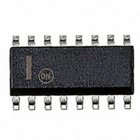
MC34025DWG ON Semiconductor, MC34025DWG Datasheet

MC34025DWG
Specifications of MC34025DWG
Available stocks
Related parts for MC34025DWG
MC34025DWG Summary of contents
Page 1
... Error Amp Noninverting Input 14 3 Error Amp Output Output Clock Power Ground Output Ground Ramp Current Limit Soft-Start Shutdown (Top View) ORDERING INFORMATION and soldering details, please download the ON Semiconductor Soldering and Mounting Techniques Reference Manual, SOLDERRM/D. Publication Order Number: MC34025/D ...
Page 2
MAXIMUM RATINGS Rating Power Supply Voltage Output Driver Supply Voltage Output Current, Source or Sink (Note 1) DC Pulsed (0.5 ms) Current Sense, Soft−Start, Ramp, and Error Amp Inputs Error Amp Output and Soft−Start Sink Current Clock and R Output ...
Page 3
ELECTRICAL CHARACTERISTICS T is the operating ambient temperature range that applies [Note 4], unless otherwise noted.) A Characteristic ERROR AMPLIFIER SECTION Input Offset Voltage Input Bias Current Input Offset Current Open−Loop Voltage Gain ( 4.0 V) ...
Page 4
100 4 2 1 ...
Page 5
55° - +125°C A -15 -20 -25 - SOURCE CURRENT (mA) Source Figure 8. Reference Voltage Change versus Source Current V ...
Page 6
9.5 9.0 8.5 8.0 7.5 7.0 -55 - AMBIENT TEMPERATURE (°C) A Figure 14. Soft−Start Charge Current versus Temperature OUTPUT RISE & FALL TIME 1.0 nF LOAD 50 ns/DIV ...
Page 7
V ref 4 Clock 5 Oscillator PWM T Comparator Ramp 7 1.25 V Error Amp Output 3 Error Amp 2 + Noninverting Input Inverting Input 1 8 Soft-Start Clock Soft-Start Error ...
Page 8
The MC33025 and MC34025 series are high speed, fixed frequency, double−ended pulse width modulator controllers optimized for high frequency operation. They are specifically designed for Off−Line and DC−to−DC converter applications offering the designer a cost effective solution with minimal external ...
Page 9
If the voltage at this pin exceeds 1.4 V, the second comparator is activated. This comparator sets a latch which, in turn, causes the Soft−Start capacitor to be discharged. In this way a “hiccup” mode of recovery is possible in ...
Page 10
Pin No. DIP/SOIC Function 1 Error Amp Inverting This pin is usually used for feedback from the output of the power supply. Input 2 Error Amp This pin is used to provide a reference in which an error signal can ...
Page 11
V ref Oscillator Additional dead time can be added by the addition of a dead time resistor from See text on oscillator section for ref T more ...
Page 12
Current Sense Information This method of slope compensation is easy to implement, however noise sensitive. Capacitor C signal is added to the current signal by a voltage divider consisting of resistors R Figure 29A. Slope Compensation (Noise Sensitive) ...
Page 13
Synchronizes Both Converters to the Same Operating Frequency + 2200 4 430 MC34025 470 680 pF 562 MMBT3904 100 Provides ...
Page 14
V ref voltage mode operation, the maximum duty cycle can be clamped. By the addition of a PNP transistor to buffer the clamp voltage, the Soft−Start current is not affected ...
Page 15
Figure 37. Application Circuit http://onsemi.com 15 ...
Page 16
Figure 38. PC Board With Components 6.5″ (Top View) http://onsemi.com 16 1500 pF 4.0″ 1500 ...
Page 17
View) 6.5″ (Bottom View) Figure 39. PC Board Without Components http://onsemi.com 17 4.0″ ...
Page 18
... ORDERING INFORMATION Device MC33025DWG MC33025DWR2G MC33025PG MC34025DWG MC34025DWR2G MC34025PG †For information on tape and reel specifications, including part orientation and tape sizes, please refer to our Tape and Reel Packaging Specifications Brochure, BRD8011/D. Package SOIC−16WB (Pb−Free) SOIC−16WB (Pb−Free) PDIP−16 (Pb−Free) SOIC− ...
Page 19
−T− 0.25 (0.010 PACKAGE DIMENSIONS PDIP−16 P SUFFIX CASE 648−08 ISSUE T L SEATING PLANE http://onsemi.com 19 NOTES: 1. ...
Page 20
... Opportunity/Affirmative Action Employer. This literature is subject to all applicable copyright laws and is not for resale in any manner. PUBLICATION ORDERING INFORMATION LITERATURE FULFILLMENT: Literature Distribution Center for ON Semiconductor P.O. Box 5163, Denver, Colorado 80217 USA Phone: 303−675−2175 or 800−344−3860 Toll Free USA/Canada Fax: 303− ...


