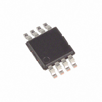
MAX5053AEUA+ Maxim Integrated Products, MAX5053AEUA+ Datasheet - Page 11

MAX5053AEUA+
Manufacturer Part Number
MAX5053AEUA+
Description
IC CNTRLR PWM CRNT MD 8-UMAX
Manufacturer
Maxim Integrated Products
Datasheet
1.MAX5053BEUA.pdf
(13 pages)
Specifications of MAX5053AEUA+
Pwm Type
Current Mode
Number Of Outputs
1
Frequency - Max
290kHz
Duty Cycle
50%
Voltage - Supply
10.8 V ~ 24 V
Buck
No
Boost
Yes
Flyback
No
Inverting
No
Doubler
No
Divider
No
Cuk
No
Isolated
Yes
Operating Temperature
-40°C ~ 85°C
Package / Case
8-MSOP, Micro8™, 8-uMAX, 8-uSOP,
Frequency-max
290kHz
Duty Cycle (max)
50 %
Output Current
1000 mA
Mounting Style
SMD/SMT
Switching Frequency
262 KHz
Maximum Operating Temperature
+ 85 C
Minimum Operating Temperature
- 40 C
Synchronous Pin
No
Topology
Boost, Flyback
Lead Free Status / RoHS Status
Lead free / RoHS Compliant
The current-sense resistor (R
the source of the MOSFET and ground, sets the current
limit. The CS input has a voltage-trip level (V
291mV. Use the following equation to calculate the
value of R
Where I
through the MOSFET.
When the voltage produced by this current (through the
current-sense resistor) exceeds the current-limit com-
parator threshold, the MOSFET driver (NDRV) quickly
terminates the current ON-cycle, typically within 60ns.
In most cases, a small RC filter is required to filter out
the leading-edge spike on the sense waveform. Set the
corner frequency at a few megahertz.
Figure 5 shows a complete design of a dual-output power
supply with a telecom voltage range of 36V to 72V. An
important aspect of this power supply is its primary-side
regulation. This regulation, through the tertiary winding,
also acts as bias winding for the MAX5052.
In the circuit of Figure 5, cross-regulation has been
improved (tertiary and 5V outputs) by using chip induc-
tors, L1 and L2, and R7||R2. R7||R2 presents enough
loading on the tertiary winding output to allow ±5% load
regulation on the 5V output over a load current range
from 150mA to 1.5A.
Figure 7. Output Voltage Regulation for the Figure 5 Circuit
Amplifier for Isolated/Nonisolated Power Supplies
PRI
CS
6.0
5.8
5.6
5.4
5.2
5.0
4.8
4.6
4.4
4.2
4.0
is the peak current in the primary that flows
0.15
:
Current-Mode PWM Controllers with an Error
Applications Information
5V OUTPUT LOAD REGULATION
0.35
______________________________________________________________________________________
Primary Regulated, Isolated
0.55
R
CS
0.75
I
Telecom Power Supply
OUT
=
V
I
(A)
PRI
CS
0.95
CS
), connected between
1.15
Current Limit
1.35
CS
) of
All printed circuit board traces carrying switching cur-
rents must be kept as short as possible, and the cur-
rent loops they form must be minimized. The pins of the
µMAX package have been placed to allow easy inter-
facing to the external MOSFET.
For universal AC input design, all applicable safety reg-
ulations must be followed. Offline power supplies may
require UL, VDE, and other similar agency approvals.
These agencies can be contacted for the latest layout
and component rules.
Typically there are two sources of noise emission in a
switching power supply: high di/dt loops and high dv/dt
surfaces. For example, traces that carry the drain cur-
rent often form high di/dt loops. Similarly, the heatsink
of the MOSFET presents a dv/dt source, thus the sur-
face area of the heatsink must be minimized as much
as possible.
To achieve best performance, a star ground connection
is recommended to avoid ground loops. For example,
the ground returns for the power-line input filter, power
MOSFET switch, and sense resistor should be routed
separately through wide copper traces to meet at a sin-
gle-system ground connection.
TRANSISTOR COUNT: 1449
PROCESS: BiCMOS
Figure 8. 12V to 15V Out Boost Regulator
0V
12V
C1
C2
C3
V
V
COMP
FB
IN
CC
MAX5053
Layout Recommendations
UVLO/EN
NDRV
GND
CS
R2
R3
Chip Information
L1
Q1
R1
D1
C4
15V
R5
R6
11


