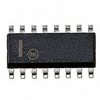
NCP1396ADR2G ON Semiconductor, NCP1396ADR2G Datasheet - Page 5

NCP1396ADR2G
Manufacturer Part Number
NCP1396ADR2G
Description
IC CTRLR OVP HV 16SOIC
Manufacturer
ON Semiconductor
Type
High Performance Resonant Mode Controllersr
Datasheet
1.NCP1396BDR2G.pdf
(25 pages)
Specifications of NCP1396ADR2G
Pwm Type
Voltage Mode
Number Of Outputs
1
Frequency - Max
575kHz
Duty Cycle
52%
Voltage - Supply
10.5 V ~ 20 V
Buck
No
Boost
No
Flyback
No
Inverting
No
Doubler
No
Divider
No
Cuk
No
Isolated
Yes
Operating Temperature
-40°C ~ 125°C
Package / Case
16-SOIC (3.9mm Width, 15 Leads)
Frequency-max
575kHz
Number Of Pwm Outputs
1
On/off Pin
No
Adjustable Output
No
Switching Freq
58.2 TO 575kHz
Operating Supply Voltage (max)
20V
Output Current
1000A
Synchronous Pin
No
Rise Time
40ns
Fall Time
20ns
Operating Temperature Classification
Automotive
Mounting
Surface Mount
Pin Count
15
Package Type
SOIC
Output Voltage Range
20 V
Power Dissipation
42 mW
Operating Temperature Range
- 40 C to + 125 C
Mounting Style
SMD/SMT
Input Voltage
12V
Frequency
500kHz
Supply Voltage Range
20V
Digital Ic Case Style
SOIC
No. Of Pins
16
Svhc
No SVHC (15-Dec-2010)
Base Number
1396
Rohs Compliant
Yes
Lead Free Status / RoHS Status
Lead free / RoHS Compliant
Other names
NCP1396ADR2GOSTR
Available stocks
Company
Part Number
Manufacturer
Quantity
Price
Company:
Part Number:
NCP1396ADR2G
Manufacturer:
ON
Quantity:
128
Part Number:
NCP1396ADR2G
Manufacturer:
ON/安森美
Quantity:
20 000
Turn- -on threshold level, V
Turn- -on threshold level, V
Minimum operating voltage after turn- -on
Startup voltage on the floating section
Cutoff voltage on the floating section
Startup current, V
V
Internal IC consumption, no output load on pin 15/14 – 11/10, Fsw =
300 kHz
Internal IC consumption, 1 nF output load on pin 15/14 – 11/10, Fsw =
300 kHz
Consumption in fault mode (All drivers disabled, V
Minimum switching frequency, Rt = 18 kΩ on pin 4, Vpin 6 = 0.8 V, DT =
300 ns
Maximum switching frequency, Rfmax = 1.3 kΩ on pin 2, Vpin 6 > 5.3 V,
Rt = 18 kΩ, DT = 300 ns
Feedback pin swing above which Δf = 0
Operating duty- -cycle symmetry
Delay before any driver re- -start in fault mode
Internal pull- -down resistor
Voltage on pin 6 below which the FB level has no VCO action
Voltage on pin 6 below which the controller considers a fault
Output voltage rise- -time @ CL = 1 nF, 10- -90% of output signal
Output voltage fall- -time @ CL = 1 nF, 10- -90% of output signal
Source resistance
Sink resistance
Dead time with R
Maximum dead- -time with R
Minimum dead- -time, R
Leakage current on high voltage pins to GND
ELECTRICAL CHARACTERISTICS
(For typical values T
SUPPLY SECTION
VOLTAGE CONTROL OSCILLATOR (VCO)
FEEDBACK SECTION
DRIVE OUTPUT
CC
level at which the internal logic gets reset
DT
CC
= 10 kΩ from pin 7 to GND
J
< VCC
= 25C, for min/max values T
DT
= 3 kΩ from pin 7 to GND
CC
CC
ON
DT
going up – A version
going up – B version
Characteristic
Characteristic
Characteristic
Characteristic
= 82 kΩ from pin 7 to GND
CC
J
= - -40C to +125C, Max T
> V
- -40C < T
0C < T
CC(min)
http://onsemi.com
)
J
J
< +125C
< +125C
5
15- -14/1
15- -14/1
15- -14/1
15- -14/1
16- -14
16- -14
11- -15
15,16
1- -10
1- -10
1- -10
1- -10
J
Pin
Pin
Pin
Pin
14,
12
12
12
12
12
12
12
12
4
2
6
6
6
6
7
7
7
= 150C, V
- -
T_dead- -max
T_dead- -min
IHV_LEAK
Vboot
VCC
VCC
Fsw max
Vboot
Fsw min
Vfb_min
Symbol
Symbol
Symbol
Symbol
VCC
VCC
Istartup
T_dead
Vfb_off
FBSW
ICC1
ICC2
ICC3
CC
Tdel
R
R
Rfb
DC
T
T
OH
OL
(min)
reset
r
f
= 12 V, unless otherwise noted.)
(min)
ON
ON
ON
12.3
58.2
Min
Min
425
Min
Min
250
9.5
8.5
7.4
48
8
- -
- -
- -
- -
- -
- -
- -
- -
- -
- -
- -
- -
- -
- -
- -
- -
- -
- -
13.4
10.5
Typ
Typ
500
Typ
Typ
300
100
9.5
8.4
6.5
1.2
5.3
1.2
0.6
5.5
11
60
50
20
20
40
20
13
9
- -
- -
4
2
- -
Max
14.3
11.5
10.5
Max
61.8
Max
Max
300
350
575
340
9.4
10
52
5
- -
- -
- -
- -
- -
- -
- -
- -
- -
- -
- -
- -
- -
- -
- -
Unit
Unit
Unit
Unit
kHz
kHz
mA
mA
mA
kΩ
mA
mA
ms
ns
ns
ns
ms
ns
%
Ω
Ω
V
V
V
V
V
V
V
V
V


