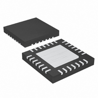
MAX8632ETI+ Maxim Integrated Products, MAX8632ETI+ Datasheet - Page 16

MAX8632ETI+
Manufacturer Part Number
MAX8632ETI+
Description
IC PWR SUPPLY DDR 28-TQFN
Manufacturer
Maxim Integrated Products
Specifications of MAX8632ETI+
Applications
Controller, DDR
Voltage - Input
2 ~ 28 V
Number Of Outputs
1
Voltage - Output
1.8V, 2.5V, 0.7 ~ 5.5 V
Operating Temperature
-40°C ~ 85°C
Mounting Type
Surface Mount
Package / Case
28-TQFN Exposed Pad
Output Voltage
1.8 V or 2.5 V or 0.7 V to 5.5 V
Output Current
15 A
Input Voltage
2 V to 28 V
Supply Current
25 uA
Switching Frequency
600 KHz
Mounting Style
SMD/SMT
Maximum Operating Temperature
+ 85 C
Minimum Operating Temperature
- 40 C
Lead Free Status / RoHS Status
Lead free / RoHS Compliant
low when SHDN is low and during the buck regulator
output’s soft-start. After the digital soft-start terminates,
POK1 becomes high impedance as long as the output
voltage is within ±10% of the nominal regulation voltage
set by FB. When V
above the nominal regulation voltage, the MAX8632
pulls POK1 low. Any fault condition forces POK1 low
until the fault latch is cleared by toggling SHDN or
cycling AV
voltages, connect an external pullup resistor between
POK1 and AV
applications. Note that the POK1 window detector is
completely independent of the overvoltage- and under-
voltage-protection fault detectors and the state of VTTS
and VTTR.
The SHDN input corresponds to the buck regulator and
places the buck regulator’s portion of the IC in a low-
power mode (see the Electrical Characteristics table).
SHDN is also used to reset a fault signal such as an
overvoltage or undervoltage fault.
When output discharge is enabled, (OVP/UVP = AV
or open) and SHDN is pulled low, or if UVP is enabled
(OVP/UVP = AV
tion set point, the MAX8632 discharges the buck regu-
lator output (through the OUT input) through an internal
10Ω switch to ground. While the output is discharging,
DL is forced low and the PWM controller is disabled but
the reference remains active to provide an accurate
threshold. Once the output voltage drops below 0.1V,
the MAX8632 shuts down the reference and DL
remains low.
When output discharge is disabled (OVP/UVP = REF or
GND), the controller does not actively discharge the
buck output and the DL driver remains low. Under these
conditions, the buck output discharge rate is deter-
minedby the load current and its output capacitance.
The buck regulator detects and latches the discharge-
mode state set by the OVP/UVP setting on startup.
Integrated DDR Power-Supply Solution for
Desktops, Notebooks, and Graphic Cards
Table 2. Shutdown and Standby Control Logic
*For DDR application, this is referred as S0 state, where all outputs are on.
**For DDR application, this is referred as S3 state, where V
***For DDR application, this is referred as S4/S5 states, where all outputs are off. Discharge mode should be selected (OVP/UVP =
AV
16
DD
GND***
AV
______________________________________________________________________________________
SHDN
AV
or OPEN, see Table 3) to discharge the outputs.
DD
DD
**
*
DD
DD
power below 1V. For logic-level output
DD
. A 100kΩ resistor works well in most
) and V
SHDN and Output Discharge
OUT
GND**
AV
STBY
X
DD
drops 10% below or rises 10%
*
OUT
falls to 70% of its regula-
BUCK OUTPUT (V
OFF
ON
ON
DDQ
DDQ
DD
)
and VTTR are kept on, but VTT is turned off (high impedance).
When OUT is discharging, both VTT and VTTR outputs
remain alive and continue to track REFIN until OUT
drops to 0.1V.
The STBY input is an active-low input that is used to
shut down only the VTT output. When STBY is low, VTT
is high impedance.
POK2 is the open-drain output for a window compara-
tor that continuously monitors the VTTS input and VTTR
output. POK2 is pulled low when REFIN is less than
0.8V. POK2 is high impedance as long as the output
voltage is within ±10% of the nominal regulation voltage
as set by REFIN. When V
above or 10% below its nominal regulation voltage, the
MAX8632 pulls POK2 low. For logic-level output volt-
ages, connect an external pullup resistor between
POK2 and AV
applications.
The VTT output is a linear regulator that regulates the
input (VTTI) to half the V
point for VTT is at the VTTS input (Figure 1). VTT is
capable of sinking and sourcing at least 1.5A of continu-
ous current and 3A peak current. The current limit for
VTT and VTTR is typically ±5A and ±32mA, respective-
ly. When the current limit for either output is reached,
the outputs regulate the current, not the voltage.
The MAX8632 provides overvoltage/undervoltage fault
protection in the buck controller. Select OVP/UVP to
enable and disable fault protection as shown in Table 3.
Once activated, the controller continuously monitors the
output for undervoltage and overvoltage fault conditions.
OFF (tracking 0.5 REFIN)
OFF (high impedance)
VTT
ON
DD
. A 100kΩ resistor works well in most
Current Limit (LDO for VTT
REFIN
VTTS
OFF (tracking 0.5 REFIN)
voltage. The feedback
Power-OK (POK2)
and VTTR Buffer)
or V
Fault Protection
VTTR
VTTR
ON
ON
rises 10%
STBY


