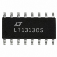
LT1313CS Linear Technology, LT1313CS Datasheet - Page 5

LT1313CS
Manufacturer Part Number
LT1313CS
Description
IC DRV/REG PCMCIA VPP DUAL16SOIC
Manufacturer
Linear Technology
Datasheet
1.LT1313CS.pdf
(12 pages)
Specifications of LT1313CS
Applications
PCMCIA Driver/Regulator, PCMCIA Card Slot
Voltage - Input
13 ~ 20 V
Number Of Outputs
2
Voltage - Output
3.3V, 5V, 12V
Operating Temperature
0°C ~ 70°C
Mounting Type
Surface Mount
Package / Case
16-SOIC (3.9mm Width)
Lead Free Status / RoHS Status
Contains lead / RoHS non-compliant
Other names
LT1313CS8
LT1313CS8
LT1313CS8
Available stocks
Company
Part Number
Manufacturer
Quantity
Price
Part Number:
LT1313CS
Manufacturer:
LINEAR/凌特
Quantity:
20 000
Part Number:
LT1313CS#PBF
Manufacturer:
LINEAR/凌特
Quantity:
20 000
Part Number:
LT1313CS#TRPBF
Manufacturer:
LINEAR/凌特
Quantity:
20 000
Supply Pins: Power is supplied to the device through the
two supply pins which must be connected together at all
times . The supply pins should be bypassed to ground if
the device is more than six inches away from the main
supply capacitor. A bypass capacitor in the range of 0.1 F
to 1 F is sufficient. The supply voltage to the LT1313 can
be loosely regulated between 13V and 20V.
VPP
two PCMCIA card VPP pins which are typically tied to-
gether at the socket. Each VPP
to approximately 330mA. Thermal shutdown provides a
second level of protection. A 1 F to 10 F tantalum output
capacitor is recommended.
Input Enable Pins: The four digital input pins are high
impedance inputs with approximately 20 A input current
at 2.4V. The input thresholds are compatible with CMOS
controllers and can be driven from either 5V or 3.3V CMOS
logic. ESD protection diodes limit input excursions to 0.6V
below ground.
PIN
BLOCK
U
OUT
FUNCTIONS
Pins: Each regulated output supplies power to the
XV
CC
U
SENSE
DIAGRAM
XEN0
XEN1
X = A OR B
V
S
4V
U
+
–
W
OUT
(One Channel)
output is current limited
LOGIC CONTROL
LOW DROPOUT
REGULATOR
VOLTAGE
LINEAR
VALID Output Pins: These pins are open-collector NPN
outputs which are driven low when the corresponding
VPP
external 51k pull-up resistors are connected between
these outputs and the same 5V or 3.3V logic supply
powering the PCMCIA compatible control logic.
V
references automatically switch the VPP
5V to 3.3V depending upon the voltage sensed at the
corresponding PCMCIA card socket V
current for these pins is approximately 30 A. For 5V only
operation, connect the Sense pins directly to ground. An
ESD protection diode limits the input voltage to 0.6V below
ground.
Ground Pins: The two ground pins must be connected
together at all times.
CC
OUT
Sense Pins: Two independent comparators and 4V
11V
pin is in regulation, i.e., when it is above 11V. Two
+
–
XVPP
XVALID
CC
1313 BD
OUT
OUT
pin. The input
outputs from
LT1313
5


