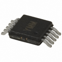
MIC5163YMM Micrel Inc, MIC5163YMM Datasheet - Page 10

MIC5163YMM
Manufacturer Part Number
MIC5163YMM
Description
IC REG CTLR DUAL MEM TERM 10MSOP
Manufacturer
Micrel Inc
Datasheet
1.MIC5163YMM.pdf
(15 pages)
Specifications of MIC5163YMM
Applications
Controller, DDR3, GDDR3/4/5
Voltage - Input
0.75 ~ 6 V
Number Of Outputs
1
Voltage - Output
Programmable
Operating Temperature
-40°C ~ 125°C
Mounting Type
Surface Mount
Package / Case
10-MSOP, Micro10™, 10-uMAX, 10-uSOP
Lead Free Status / RoHS Status
Lead free / RoHS Compliant
Other names
576-3482-5
Available stocks
Company
Part Number
Manufacturer
Quantity
Price
Part Number:
MIC5163YMM TR
Manufacturer:
MICREL/麦瑞
Quantity:
20 000
Application Information
Synchronous
(SDRAM) has continually evolved over the years to keep
up with ever-increasing computing needs. The latest
addition to SDRAM technology is DDR3 SDRAM. DDR3
SDRAM is the third generation of the DDR SDRAM
family and offers improved power savings, higher data
bandwidth and enhanced signal quality with multiple on-
die termination (ODT) selection. In DDR3 SDRAM the
values of the ODT are based on the value of an external
resistor. In addition to using this external resistor for
setting the ODT value, it is also used for calibrating the
ODT value so that it maintains its resistance value to
within a 10% tolerance.
To improve signal integrity and support higher frequency
operations, the JEDEC committee defined a fly-by
termination scheme used with the clocks, the command
bus and address bus signals. The fly-by topology
reduces
deliberately causing flight-time skew between the data
and strobes at every DRAM as the clock, address and
command signals traverse the DIMM.
output buffer. Currently, there are two drive strength
settings, 34Ω and 40Ω. The 40Ω drive strength setting is
currently a reserved specification defined by JEDEC, but
available on the DDR3 SDRAM.
The MIC5163 is a high performance linear controller that
utilizes scalable N-Channel MOSFETs to provide
JEDEC compliant bus termination. Termination is
achieved by dividing down the V
provide the reference (V
amplifier compares the termination voltage (V
V
sink and/or source current to maintain a termination
voltage (V
their enhancement voltage from a separate V
the device. Although the general discussion is focused
The DDR3 SDRAM uses a programmable impedance
Micrel, Inc.
April 2009
REF
, controlling two external N-Channel MOSFETs to
Receiver
Receiver
Driver
Driver
Figure 3. Dynamic OCT between Stratix III/IV
simultaneous
TT
) equal to V
FPGA
FPGA
Dynamic
V
V
REF
REF
= 0.75V
= 0.75V
FPGA Devices
3” Trace Length
3” Trace Length
REF
switching
REF
Random
) voltage. An internal error
. The N-Channels receive
V
V
REF
REF
DDQ
= 0.75V
= 0.75V
noise
voltage by half to
Access
DDR3 DIMM
R
DDR3 DIMM
R
S
S
DDR3 Component
DDR3 Component
(SSN)
CC
Receiver
Receiver
Memory
TT
Driver
Driver
pin on
) and
by
10
on DDR3, the MIC5163 is also capable of providing bus
terminations for DDR, DDR2 and GDDR3/4/5.
V
The V
current through the high side N-Channel and the
reference voltage to the device. The MIC5163 can
operate at V
possibility of large transient currents being sourced from
this line, significant bypass capacitance will increase
performance by improving the source impedance at
higher frequencies. Since the reference is simply V
perturbations on the V
amplitude on the reference. For this reason, low ESR
capacitors
recommended on V
V
V
V
by V
large signal transient response, Oscons and ceramics
are recommended on V
placement of the Oscon and ceramic capacitors is
important to reduce both ESR and ESL such that high-
current high-speed transients do not exceed the dynamic
voltage tolerance requirement of V
capacitors provide bulk charge storage while the smaller
ceramic capacitors provide current during the fast edges
of the bus transition. Using several smaller ceramic
capacitors distributed near the termination resistors is
typically important to reduce the effects of PCB trace
inductance.
V
Two resistors dividing down the V
V
17kΩ. A minimum capacitor value of 120pF from V
ground is required to remove high frequency signals
reflected from the source. Large capacitance values
(>1500pF) should be avoided. Values greater than
1500pF slow down V
voltage’s ability to track V
transients.
100µF
Figure 4. MIC5163 as a DDR3 Memory Termination Device
V
6.3V
DDQ
TT
TT
REF
REF
REF
DDQ
GND
= 1.2V
is the actual termination point. V
. Due to high speed signaling, the load current seen
TT
100µF
(Figure 5). The resistors are valued at around
6.3V
DDQ
is constantly changing. To maintain adequate
1µF
10V
V
CC
pin on the MIC5163 provides the source
= 5V
DDQ
such
120pF
EN
voltages as low as 0.75V. Due to the
DDQ
for 7A Application
U1
MIC5163
VCC
EN
VREF
as
REF
VDDQ
.
GND
DDQ
TT
COMP
and detract from the reference
HSD
LSD
ceramics
. The proper combination and
FB
DDQ
will also appear at half the
220pF
during high speed load
DDQ
or
TT
TT
M9999-042209-A
SUD50N02-06P
voltage provide
is regulated to
. The Oscon
Oscons
100µF
6.3V
MIC5163
DDQ
REF
V
TT
100µF
6.3V
GND
= 0.6V
are
/2,
to


