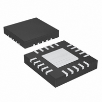
MAX1515ETG+ Maxim Integrated Products, MAX1515ETG+ Datasheet

MAX1515ETG+
Specifications of MAX1515ETG+
Related parts for MAX1515ETG+
MAX1515ETG+ Summary of contents
Page 1
... Shutdown Supply Current ♦ < 800µA (max) Operating Supply Current ♦ Selectable Pulse-Skipping Operation at Light Loads ♦ Positive and Negative Current Limit ♦ Power-Good Window Comparator ♦ Output Short-Circuit Protection PART MAX1515ETG MAX1515ETG+ +Denotes lead-free package. (3.0V TO 3.6V) Applications V DDQ (2.5V OR 1.8V) Features ...
Page 2
Low-Voltage, Internal Switch, Step-Down/DDR Regulator ABSOLUTE MAXIMUM RATINGS , LX, SHDN to GND ...................................-0. MODE GND ....................................................-0.3V to +4V COMP, FB, REF, REFIN, REFOUT, PGOOD to GND.........................................................-0. FBSEL0, FBSEL1, ...
Page 3
ELECTRICAL CHARACTERISTICS (continued) (Circuit of Figure +3.3V erwise noted. Typical values are +25°C.) A PARAMETER SYMBOL Sink-Mode Detect Threshold Source-Mode Detect Threshold MOSFET On-Resistance Switching Frequency Maximum Output Current ...
Page 4
Low-Voltage, Internal Switch, Step-Down/DDR Regulator ELECTRICAL CHARACTERISTICS (continued) (Circuit of Figure +3.3V erwise noted. Typical values are +25°C.) A PARAMETER SYMBOL REFERENCE Reference Voltage V Reference Load Regulation REFIN ...
Page 5
ELECTRICAL CHARACTERISTICS (Circuit of Figure +3.3V otherwise noted. Note 5) PARAMETER SYMBOL PWM CONTROLLER Input Voltage Range V Output Adjust Range Feedback Voltage Accuracy Sink-Mode Detect Threshold Source-Mode Detect Threshold nFET On-Resistance Switching Frequency ...
Page 6
Low-Voltage, Internal Switch, Step-Down/DDR Regulator ELECTRICAL CHARACTERISTICS (continued) (Circuit of Figure +3.3V otherwise noted. Note 5) PARAMETER SYMBOL I CC No-Load Supply Current + Shutdown Supply Currents ...
Page 7
Circuit of Figure 2.5V 1.25V OUTPUT EFFICIENCY vs. LOAD CURRENT 100 SOURCE, SKIP 90 80 SINK, SKIP SOURCE, PWM 40 SINK, PWM 2. 1.25V ...
Page 8
Low-Voltage, Internal Switch, Step-Down/DDR Regulator (MAX1515 Circuit of Figure 2.5V REF VOLTAGE vs. REF LOAD CURRENT 1.104 1.102 1.100 1.098 1.096 100 REF LOAD CURRENT (μA) PEAK CURRENT LIMIT vs. ...
Page 9
Circuit of Figure 2.5V STARTUP AND SHUTDOWN WAVEFORM (LIGHT LOAD) 3. 1.25V 0 SKIP = GND, R LOAD 1ms/div A: PGOOD, 5V/div D: INDUCTOR CURRENT, 1A/div B: SS, 2V/div ...
Page 10
Low-Voltage, Internal Switch, Step-Down/DDR Regulator (MAX1515 Circuit of Figure 2.5V DDR-MODE LOAD TRANSIENT 2. -2A 1.25V 20μs/div A: LX, 2V/div C: INDUCTOR CURRENT, 2A/div B: LOAD CONTROL, D: OUTPUT VOLTAGE, 50mV/div ...
Page 11
PIN NAME Power Ground. Internal connection to the source of the internal synchronous-rectifier switch. Connect 1, 2 PGND both PGND pins together Internally Connected Pin. Connect to PGND. Supply Input for the Low-Side Gate Drive and REFOUT Buffer. ...
Page 12
Low-Voltage, Internal Switch, Step-Down/DDR Regulator PIN NAME Used with FBSEL0 to set the output voltage of the step-down regulator when MODE = GND. 18 FBSEL1 Connect to GND if MODE = V Pulse-Skipping Control Input. Connect to V SKIP 19 ...
Page 13
V BIAS (3.0V TO 3.6V) R2 100kΩ PWM MODE SKIP MODE ON OFF (DDR MODE) R3 10kΩ V DDQ 1% (2.5V OR 1.8V) Figure 1. Standard Application Circuit REF REF FB GAIN GND 1.1V PGOOD PGOOD LOGIC ...
Page 14
Low-Voltage, Internal Switch, Step-Down/DDR Regulator +3.3V Bias Supply (V The MAX1515 requires a 3.3V bias supply for its inter- nal circuitry. Typically, this 3.3V bias supply is the note- book’s 95%-efficient, 3.3V system supply. The 3.3V bias supply must provide ...
Page 15
SHDN 0. (A) LIMIT Figure 3. Soft-Start Current Limit Short-Circuit/Overload Protection The MAX1515 can sustain a constant short circuit or overload. Under a source-mode short-circuit or over- load condition, when V < 0 ...
Page 16
Low-Voltage, Internal Switch, Step-Down/DDR Regulator Table 3. Modes of Operation MODE SHDN SKIP PIN Low Low X Low High X High Low Low High Low High High High Low High High High X = Don’t care. Pulse Skipping (Source Mode) ...
Page 17
REF and ground (Figure 5). Regulation is maintained for adjustable output voltages when Use 100kΩ for R FB REFIN the equation: ⎛ ⎜ FB REF + ⎝ R ...
Page 18
Low-Voltage, Internal Switch, Step-Down/DDR Regulator MAXIMUM RECOMMENDED OPERATING FREQUENCY vs. INPUT VOLTAGE 1000 V OUT 800 600 400 V = 1.5V OUT V = 1.25V OUT 200 V OUT 0 1.5 2.0 2.5 3.0 V (V) IN Figure 6. Maximum ...
Page 19
While sourcing current, V and V CHG with source load current and the voltage across the inductor decreases. This causes the frequency to drop. Conversely, while sinking current, V decrease with sink load current and the voltage across the inductor ...
Page 20
Low-Voltage, Internal Switch, Step-Down/DDR Regulator The actual capacitance value required relates to the physical size needed to achieve low ESR, as well as to the chemistry of the capacitor technology. Thus, the capacitor is usually selected by ESR and voltage ...
Page 21
V SKIP CC REF MAX1515 R1 C REFIN REFIN R2 V OUT(LOW OUT(HIGH) Figure 7. Dynamic Output Voltages voltage-divider network at REFIN. The resulting output voltages are determined by the following equations: ⎛ ⎜ OUT ...
Page 22
Low-Voltage, Internal Switch, Step-Down/DDR Regulator Pin Configuration TOP VIEW SKIP 19 BST MAX1515 THIN QFN (4mm x 4mm) 22 ______________________________________________________________________________________ 13 ...
Page 23
For the latest package outline information go to www.maxim-ic.com/packages.) ______________________________________________________________________________________ Low-Voltage, Internal Switch, Step-Down/DDR Regulator Package Information PACKAGE OUTLINE, 12, 16, 20, 24, 28L THIN QFN, ...
Page 24
... Maxim cannot assume responsibility for use of any circuitry other than circuitry entirely embodied in a Maxim product. No circuit patent licenses are implied. Maxim reserves the right to change the circuitry and specifications without notice at any time. 24 ____________________Maxim Integrated Products, 120 San Gabriel Drive, Sunnyvale, CA 94086 408-737-7600 © 2006 Maxim Integrated Products Package Information (continued) Printed USA is a registered trademark of Maxim Integrated Products, Inc ...


