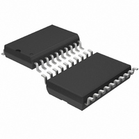
LTC1553CSW Linear Technology, LTC1553CSW Datasheet - Page 6

LTC1553CSW
Manufacturer Part Number
LTC1553CSW
Description
IC SW REG CNTRLR 5BIT PROG20SOIC
Manufacturer
Linear Technology
Datasheet
1.LTC1553CSW.pdf
(24 pages)
Specifications of LTC1553CSW
Applications
Controller, Intel Pentium® II
Voltage - Input
5V, 12V
Number Of Outputs
1
Voltage - Output
1.8 ~ 3.5 V
Operating Temperature
0°C ~ 70°C
Mounting Type
Surface Mount
Package / Case
20-SOIC (7.5mm Width)
Lead Free Status / RoHS Status
Contains lead / RoHS non-compliant
Available stocks
Company
Part Number
Manufacturer
Quantity
Price
Part Number:
LTC1553CSW
Manufacturer:
LT/凌特
Quantity:
20 000
LTC1553
PIN
G2 (Pin 1): Gate Drive for the Lower N-Channel MOSFET,
Q2. This output will swing from PV
be low when G1 is high or when the output is disabled. To
prevent undershoot during a soft start cycle, G2 is held low
until G1 first goes high.
PV
connected to a potential of at least V
V
pump connected to the switching node between Q1 and
Q2 (see Figure 7), or it can be connected to an auxiliary 12V
supply if one exists. For applications where V
PV
Figure 9).
GND (Pin 3): Power Ground. GND should be connected to
a low impedance ground plane in close proximity to the
source of Q2.
SGND (Pin 4): Signal Ground. SGND is connected to the
low power internal circuitry and should be connected to
the negative terminal of the output capacitor where it
returns to the ground plane. GND and SGND should be
shorted right at the LTC1553.
V
power circuity. V
drain of Q1 if they share the same supply. A 10 F bypass
capacitor is recommended from this pin to SGND.
SENSE (Pin 6): Output Voltage Pin. Connect to the positive
terminal of the output capacitor. There is an internal 120k
resistor connected from this pin to SGND. SENSE is a very
sensitive pin; for optimum performance, connect an exter-
nal 0.1 F capacitor from this pin to SGND. By connecting
a small external resistor between the output capacitor and
the SENSE pin, the initial output voltage can be raised
slightly. Since the internal divider has a nominal imped-
ance of 120k , a 1200
nominal output voltage by 1%. If an external resistor is
used, the value of the 0.1 F capacitor on the SENSE pin
must be greatly reduced or loop phase margin will suffer.
Set a time constant for the RC combination of approxi-
mately 0.1 s. So, for example, with a 1200 resistor, set
C = 83pF. Use a standard 100pF capacitor.
6
IN
CC
CC
CC
U
= 5V, PV
(Pin 5): Power Supply. Power for the internal low
(Pin 2): Power Supply for G1 and G2. PV
can be generated using a 17V charge pump (see
FUNCTIONS
U
CC
can be generated using a simple charge
CC
should be wired separately from the
U
series resistor will raise the
CC
to GND. It will always
IN
+ V
GS(ON)Q1
CC
IN
must be
= 12V,
. If
I
by the voltage drop across an external resistor connected
between the drain of Q1 and I
pull-down at I
I
switching node between the source of Q1 and the drain of
Q2. If I
will go into current limit. The current limit circuit can be
disabled by floating I
an external 10k resistor. For V
from I
spike at I
SS (Pin 9): Soft Start. Connect to an external capacitor to
implement a soft start function. During moderate overload
conditions, the soft start capacitor will be discharged
slowly in order to reduce the duty cycle. In hard current
limit, the soft start capacitor will be forced low immedi-
ately and the LTC1553 will rerun a complete soft start
cycle. C
current through Q1 will not exceed the current limit value.
COMP (Pin 10): External Compensation. The COMP pin is
connected directly to the output of the error amplifier and
the input of the PWM comparator. An RC + C network is
used at this node to compensate the feedback loop to
provide optimum transient response.
OT (Pin 11): Over-Temperature Fault. OT is an open-drain
output and will be pulled low if OUTEN is less than 2V. If
OUTEN = 0, OT pulls low.
FAULT (Pin 12): Overvoltage Fault. FAULT is an open-
drain output. If V
output voltage, FAULT will go low and G1 and G2 will be
disabled. Once triggered, the LTC1553 will remain in this
state until the power supply is recycled or the OUTEN pin
is toggled. If OUTEN = 0, FAULT floats or is pulled high by
an external resistor.
PWRGD (Pin 13): Power Good. This is an open-drain
signal to indicate validity of output voltage. A high indi-
cates that the output has settled to within 5% of the rated
output for more than 1ms. PWRGD will go low if the output
is out of regulation for more than 500 s. If OUTEN = 0,
PWRGD pulls low.
MAX
FB
(Pin 8): Current Limit Sense Pin. Connect to the
(Pin 7): Current Limit Threshold. Current limit is set
FB
FB
SS
to GND is recommended to prevent the voltage
FB
drops below I
must be selected such that during power-up the
from exceeding the maximum voltage rating.
MAX
.
OUT
MAX
reaches 15% above the nominal
MAX
and shorting I
MAX
when G1 is on, the LTC1553
IN
. There is a 180 A internal
= 12V, a 15V Zener diode
FB
to V
CC
through


