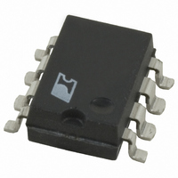
DPA423G-TL Power Integrations, DPA423G-TL Datasheet - Page 5

DPA423G-TL
Manufacturer Part Number
DPA423G-TL
Description
IC CONV DC-DC DPA SWITCH 8SMD
Manufacturer
Power Integrations
Series
DPA-Switch®r
Specifications of DPA423G-TL
Applications
Converter, Power Over Ethernet and Telecom Applications
Voltage - Input
16 ~ 75 V
Number Of Outputs
1
Voltage - Output
220V
Operating Temperature
-40°C ~ 125°C
Mounting Type
Surface Mount
Package / Case
8-SMD Gull Wing
For Use With
596-1195 - KIT REF DES DPA 6.6W DC-DC CONV596-1009 - KIT DESIGN ACCELERATOR DC-DC596-1007 - KIT DESIGN ACCELERATOR POE CONV
Lead Free Status / RoHS Status
Request inventory verification / RoHS non-compliant
overloaded output exists, the feedback loop will close, providing
external CONTROL pin current, before the CONTROL pin
voltage has had a chance to discharge to the lower threshold
voltage of approximately 4.8 V (internal supply undervoltage
lockout threshold). When the externally fed current charges the
CONTROL pin to the shunt regulator voltage of 5.8 V, current in
excess of the consumption of the chip is shunted to SOURCE
through resistor R
through R
provide closed loop regulation. The shunt regulator has a fi nite
low output impedance Z
when used in a primary feedback confi guration. The dynamic
impedance Z
CONTROL pin capacitance sets the dominant pole for the
control loop.
When a fault condition such as an open loop or overloaded
output prevents the fl ow of an external current into the
CONTROL pin, the capacitor on the CONTROL pin discharges
towards 4.8 V. At 4.8 V auto-restart is activated which turns the
output MOSFET off and puts the control circuitry in a low
current standby mode. The high-voltage current source turns
on and charges the external capacitance again. A hysteretic
internal supply under-voltage comparator keeps V
window of typically 4.8 V to 5.8 V by turning the high-voltage
current source on and off as shown in Figure 5. The auto-
restart circuit has a divide-by-8 counter that prevents the output
MOSFET from turning on again until eight discharge/charge
cycles have elapsed. This is accomplished by enabling the
output MOSFET only when the divide-by-8 counter reaches full
count (S7). The counter effectively limits DPA-Switch power
dissipation as well as the maximum power delivered to the
power supply output by reducing the auto-restart duty cycle to
typically 4%. Auto-restart mode continues until output voltage
regulation is again achieved through closure of the feedback
loop.
Figure 5.
www.powerint.com
V
V
V
Note: S0 through S7 are the output states of the auto-restart counter
LINE
C
DRAIN
V
0 V
0 V
0 V
0 V
OUT
Typical Waveforms for (1) Power Up, (2) Normal Operation, (3) Auto-restart and (4) Power Down.
E
controls the duty cycle of the power MOSFET to
C
V
of the CONTROL pin together with the external
UV
E
as shown in Figure 2. This current fl owing
1
S7
C
that sets the gain of the error amplifi er
S0
2
S1
S2
S6
C
within a
S7
3
S0
S1
S2
Oscillator and Switching Frequency
The internal oscillator linearly charges and discharges an
internal capacitance between two voltage levels to create a
sawtooth waveform for the pulse width modulator. The
oscillator sets both the pulse width modulator latch and the
current limit latch at the beginning of each cycle.
The nominal switching frequency of 400 kHz was chosen to
minimize the transformer size and to allow faster power supply
loop response. The FREQUENCY pin, when shorted to the
CONTROL pin, lowers the switching frequency to 300 kHz,
which may be preferable in some applications such as those
employing secondary synchronous rectifi cation. Otherwise, the
FREQUENCY pin should be connected to the SOURCE pin for
the default 400 kHz.
Pulse Width Modulator and Maximum Duty Cycle
The pulse width modulator implements voltage mode control by
driving the output MOSFET with a duty cycle inversely
proportional to the current into the CONTROL pin that is in
excess of the internal supply current of the chip (see Figure 4).
The excess current is the feedback error signal that appears
across R
with a typical corner frequency of 30 kHz to reduce the effect of
switching noise in the chip supply current generated by the
MOSFET gate driver. The fi ltered error signal is compared with
the internal oscillator sawtooth waveform to generate the duty
cycle waveform. As the control current increases, the duty cycle
decreases. A clock signal from the oscillator sets a latch that
turns on the output MOSFET. The pulse width modulator resets
the latch, turning off the output MOSFET. Note that a minimum
current must be driven into the CONTROL pin before the duty
cycle begins to change.
S6
S7
E
(see Figure 2). This signal is fi ltered by an RC network
2
S0
S1
S2
4
DPA422-426
S6
S7
S7
4.8 V
PI-3867-050602
5.8 V
Rev. S 12/07
5


