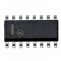
CS5157HGDR16G ON Semiconductor, CS5157HGDR16G Datasheet

CS5157HGDR16G
Specifications of CS5157HGDR16G
CS5157HGDR16GOSTR
Related parts for CS5157HGDR16G
CS5157HGDR16G Summary of contents
Page 1
... ORDERING INFORMATION Device Package CS5157HGD16 SO−16 CS5157HGD16G SO−16 (Pb−Free) CS5157HGDR16 SO−16 CS5157HGDR16G SO−16 (Pb−Free) †For information on tape and reel specifications, including part orientation and tape sizes, please refer to our Tape and Reel Packaging Specifications Brochure, BRD8011/D. 1 SOIC−16 D SUFFIX CASE 751B ...
Page 2
CC1 CC2 V V ID0 ID0 V V ID1 ID1 V V ID2 ID2 V V ID3 ID3 V V ID4 ID4 CS5157H C OFF 330 pF SS 0.1 mF COMP 0.33 mF LGND Figure 1. ...
Page 3
ELECTRICAL CHARACTERISTICS (0°C < ID4 ID2 ID1 ID0 ID3 ; GATE(L) Characteristic Error Amplifier V Bias Current Open Loop Gain 1.25 V < ...
Page 4
ELECTRICAL CHARACTERISTICS (0°C < ID4 ID2 ID1 ID0 ID3 ; GATE(L) Characteristic DAC Input Threshold V Input Pullup Resistance V Pullup Voltage Accuracy (all codes except ...
Page 5
ELECTRICAL CHARACTERISTICS (0°C < ID4 ID2 ID1 ID0 ID3 ; GATE(L) Characteristic Supply Current I No Switching CC1 I No Switching CC2 Operating I V CC1 ...
Page 6
V Monitor CC1 Comparator − V CC1 + 3.90 V 3.85V SS V ID0 Error V ID1 Amplifier 5 BIT + V DAC ID2 V − ID3 PWM Comparator V ID4 Slow Feedback V FB COMP Fast Feedback V FFB ...
Page 7
The V control method is illustrated in Figure 3. The output voltage is used to generate both the error signal and the ramp signal. Since the ramp signal is simply the output voltage affected by any change ...
Page 8
M 250 ms Trace 1− Regulator Output Voltage (1.0 V/div.) Trace 2− Inductor Switching Node (2.0 V/div.) Trace 3− Input (V and V ) (5.0 V/div.) CC1 CC2 Trace 4− 5.0 V Input (1.0 V/div.) Figure 4. CS5157H ...
Page 9
M 1.00 ms Trace 1− Regulator Output Voltage (10 mV/div.) Trace 2− Inductor Switching Node (5.0 V/div.) Figure 8. Peak−to−Peak Ripple (Heavy Load) OUT Transient Response 2 The CS5157H V control loop’s 100 ns ...
Page 10
Short Circuit Protection A lossless hiccup mode short circuit protection feature is provided, requiring only the Soft−Start capacitor to implement short circuit condition occurs (V the V low comparator sets the FAULT latch. This causes FFB the MOSFET ...
Page 11
M 5.00 ms Trace 4− 5.0 V from PC Power Supply (2.0 V/div.) Trace 1− Regulator Output Voltage (1.0 V/div.) Figure 15. OVP Response to an Input−to−Output Short Circuit by Pulling the Input Voltage to Ground External Output Enable Circuit ...
Page 12
IC. For the typical application where CC1 CC2 used as the source for the regulator output current, the following gate drive is provided; V GATE( 5.0 ...
Page 13
A heatsink may be added to TO−220 components to reduce their thermal impedance. A number of PC board layout techniques such as thermal vias and additional copper foil area can be used to improve the power handling capability of surface ...
Page 14
MBRS 120 0.1 mF MBRS120 MBRS120 1 CC1 V ID0 V ID1 V ID2 V ID3 CS5157H V ID4 C OFF 330 pF SS 0.1 mF COMP 0.33 mF Figure 23. Additional Application Diagram, 5 ...
Page 15
MBRS 120 0.1 mF MBRS120 MBRS120 1 CC1 V ID0 V ID1 V ID2 V CS5157H ID3 V ID4 C OFF 330 pF SS 0.1 mF COMP 0.33 mF Figure 25. Additional Application Diagram, 5 ...
Page 16
... SOIC−16 Typical 28 Typical 115 N. American Technical Support: 800−282−9855 Toll Free USA/Canada Japan: ON Semiconductor, Japan Customer Focus Center 2−9−1 Kamimeguro, Meguro−ku, Tokyo, Japan 153−0051 Phone: 81−3−5773−3850 http://onsemi.com 16 NOTES: 1. DIMENSIONING AND TOLERANCING PER ANSI Y14 ...


